In embedded development, registers are collections of bits. When you see that GPIOA->MODER is 0x00000400, being able to instantly read what that means — that’s the goal of this episode.
In Episode 3 we covered the memory layout of C structs, arrays, and padding. Now we build the skill to manipulate peripheral registers at the bit level with precision.
📖 Previous Article
📍 Series Index
✅ What You'll Be Able to Do After This Article
- Use bit masks and shift operations to safely manipulate specific bits in a register
- Explain the danger of the RMW (Read-Modify-Write) problem and why to avoid direct ODR writes
- Explain how BSRR provides atomic operation and why it's better than ODR
- Blink an LED with direct register access (both ODR and BSRR versions)
- Measure the execution speed difference between HAL and register access using DWT CYCCNT
Table of Contents
- Registers Are Collections of Bits
- Bit Operation Basics: Masks and Shifts
- The RMW Problem: The Pitfall of “Read, Modify, Write”
- The BSRR Philosophy: STM32’s Elegant Design
- Practice: Experience LED Blinking Three Ways
- Advanced: How RCC Clock Enable Works
- Frequently Asked Questions (FAQ)
- Episode 4 Summary
1. Registers Are Collections of Bits
1-1. Why Manage at the Bit Level?
In Episode 1, we introduced that GPIO registers have roles like MODER, OTYPER, and OSPEEDR. These registers are 32-bit (4-byte) integers, but their contents are “a collection of bit fields (functional blocks).”
Let’s review the main registers for GPIOA:
| Register | Address | Role |
|---|---|---|
| MODER | 0x40020000 | Pin mode setting (input / output / alternate function / analog) |
| OTYPER | 0x40020004 | Output type (push-pull / open-drain) |
| OSPEEDR | 0x40020008 | Output speed |
| PUPDR | 0x4002000C | Pull-up / pull-down setting |
| IDR | 0x40020010 | Input data register (read pin state) |
| ODR | 0x40020014 | Output data register (turn pin ON/OFF) |
We’ll mainly work with ODR and the BSRR that appears later. The other registers are configured by HAL during initialization — just know they exist for now.
What are “bits” and “registers”?
Inside a computer, all information is represented as combinations of 0s and 1s. The minimum unit — either 0 or 1 — is called a bit.
Think of a light switch: “OFF = 0,” “ON = 1.”
1 bit = 1 switch (2 choices: 0 or 1)

  OFF  ON
  [ 0  1 ]  ← this is 1 bit
Microcontroller CPUs operate with “32-bit width” — 32 switches bundled together. Each register has 32 switches packed inside it.
A 32-bit register = a panel with 32 switches in a row

bit31                                              bit0
 ↓                                                  ↓
[0][0][0][0][0][0][0][0][0][0][0][0][0][1][0][0][0][0][0][0][0][0][0][0][0][0][0][0][0][0][0][0]
This value in hexadecimal is 0x00001000.
This collection of 32 zeros and ones is literally what a register is. Each peripheral (GPIO, UART, timers) has dedicated registers, and which bits are 0 or 1 determines hardware behavior.
For example, GPIOA->MODER (pin mode configuration register) looks like this:
MODER register (32 bits)
bit31  bit30  ...  bit11 bit10  bit9  bit8  ...  bit1  bit0
 PA15  PA15  ...   PA5   PA5   PA4   PA4  ...   PA0   PA0
 [1]   [0]  ...   [1]   [0]   [1]   [0]  ...   [1]   [0]
Each pin gets 2 bits, and their combination sets the mode:
| Bit value | Meaning |
|---|---|
00 |
Input mode (reset state) |
01 |
General-purpose output mode |
10 |
Alternate function mode (UART, SPI, etc.) |
11 |
Analog mode |
So to set PA5 (pin 5) to output mode, we need to set bits 11–10 of MODER to 01.
“Wouldn’t rewriting all 32 bits break other settings?”
Exactly right — that’s why we need the technique of changing only specific bits. That’s the “mask operations” covered next.
1-2. The “Registers as Bit Collections” Mindset
An important shift in perspective for embedded development:
- PC programming mindset: Variables “hold numeric values”
- Embedded mindset: Registers are “a collection of configuration switches”
When you write 0x00000400 to MODER, you’re not writing “the meaningful number 400.” You’re setting “the switch state bit11:bit10 = 01.”
This ability to read and write registers as bit collections is the foundational skill of an embedded engineer.
2. Bit Operation Basics: Masks and Shifts
2-1. Shift Operations (<< and >>)
Shift operations move a bit pattern left or right.
uint32_t value = 1;     // 0b00000000000000000000000000000001

value << 1;             // 0b00000000000000000000000000000010  (2)
value << 5;             // 0b00000000000000000000000000100000  (32)
value << 10;            // 0b00000000000000000000010000000000  (1024)
1 << n creates “a value with only the nth bit set.” This lets you write specific bit positions with meaningful names:
// Bit position for PA5 (MODER uses 2 bits per pin)
#define PA5_MODER_POS  (5 * 2)      // = 10 (starts at bit10)
#define PA5_MODER_MASK (0x3UL << PA5_MODER_POS)  // place 0b11 at bit10

// "0x3UL" = 0b11 (a 2-bit-wide mask) shifted to bit10 position
// → 0x00000C00
What is the
ULsuffix? TheULin3ULmeans “unsigned long.” In bit operations, this suffix prevents undefined behavior from unintended sign bit handling during shifts.
2-2. Mask Operations (&, |, ~)
Mask operations are the fundamental technique for manipulating specific bits.
Quick Reference: Bit Logic Operations
| Operation | Symbol | Use | Example (8-bit) |
|---|---|---|---|
| AND | & |
Clear specific bits (set to 0) | 0b1010_1010 & 0b0000_1111 = 0b0000_1010 |
| OR | | |
Set specific bits (set to 1) | 0b1010_1010 | 0b0000_1111 = 0b1010_1111 |
| NOT | ~ |
Invert bits | ~0b0000_1111 = 0b1111_0000 |
| XOR | ^ |
Toggle specific bits (flip) | 0b1010_1010 ^ 0b0000_1111 = 0b1010_0101 |
Concrete Example: Setting PA5 to Output Mode
// Goal: set MODER's bit11:bit10 to 01

// Step 1: clear the target bits (AND + NOT mask)
GPIOA->MODER &= ~(0x3UL << (5 * 2));
// ~(0x3 << 10) = ~0x00000C00 = 0xFFFFF3FF
// → only zeros bit11:bit10, preserving all other bits

// Step 2: set the new value (OR)
GPIOA->MODER |= (0x1UL << (5 * 2));
// 0x1 << 10 = 0x00000400
// → sets bit10 to 1 (bit11 stays 0)
After this operation, MODER bits 11–10 = 01, setting PA5 to output mode.
2-3. Summary of Common Bit Operation Patterns
Frequently used patterns in embedded programming:
uint32_t reg = ...;      // target register

// Set a bit (to 1)
reg |= (1UL << n);       // set the nth bit to 1

// Clear a bit (to 0)
reg &= ~(1UL << n);      // clear the nth bit to 0

// Toggle a bit (0→1 / 1→0)
reg ^= (1UL << n);       // flip the nth bit

// Check a bit (is it 0 or 1?)
if (reg & (1UL << n)) {  // true if the nth bit is 1
    // ...
}

// Clear a field then set it (mask + OR)
reg &= ~(MASK << pos);   // clear the target field
reg |= (VALUE << pos);   // set the new value
✅ Chapter 2 Checklist
- Can mentally calculate what
1 << 5equals - Can write the two-step “clear bits → set bits” operation
- Understands that
~inverts bits
3. The RMW Problem: The Pitfall of “Read, Modify, Write”
3-1. What Is ODR?
A new register appears: ODR (Output Data Register).
ODR manages the output state of GPIO pins. Its 16 bits correspond to 16 pins: bit = 1 means HIGH (3.3V), bit = 0 means LOW (0V).
ODR register (lower 16 bits)

bit15  bit14  ...  bit6  bit5  bit4  ...  bit1  bit0
 PA15   PA14  ...  PA6   PA5   PA4  ...   PA1   PA0
  0      0    ...   0     0     0   ...    0     0    ← all 0 at startup
To set PA5 HIGH, we need to set only bit5 to 1:
GPIOA->ODR |= (1UL << 5);
| Part | Meaning |
|---|---|
GPIOA |
Pointer to GPIOA’s register set |
->ODR |
Access the ODR register inside it (-> is pointer-access notation) |
1UL << 5 |
Shift 1 left by 5 → only bit5 is 1 |
|= |
OR with current ODR value and write back |
Note on
->notationGPIOAis a pointer holding an address. Use->(not.) to access members through a pointer. Details in Episode 5 (Pointers).
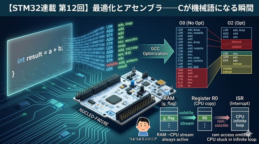
Why doesn’t the compiler optimize this away? The CMSIS register struct (
GPIO_TypeDef) is defined internally withvolatile, so the compiler cannot skip these reads/writes. Thevolatilefrom Episode 3 is at work here.
3-2. What Is RMW (Read-Modify-Write)?
The |= operation above has 3 steps under the hood:
1. Read    : load the current ODR value into the CPU
2. Modify  : compute setting bit5 to 1
3. Write   : write the result back to ODR
This is called RMW (Read-Modify-Write).
3-3. The RMW Problem
Since RMW consists of three independent operations, another process can interrupt between them.
Typical scenario:
// In the main loop, operating PA5
GPIOA->ODR |= (1UL << 5);    // want to set PA5 HIGH
// ↑ internally: read ODR → set bit5 → write ODR

// But what if an interrupt fires between "read ODR" and "write ODR"
// and modifies PA6?
Time →
[Main] Read ODR (ODR = 0x0000)          ← PA5 and PA6 both LOW
[IRQ!] ← interrupt fires
[IRQ ] ODR |= (1 << 6)  ← set PA6 HIGH (ODR = 0x0040)
[IRQ ] interrupt returns
[Main] writes back (0x0000 | 0x0020 = 0x0020)  ← PA6 change is LOST!
The interrupt’s PA6 change was overwritten and erased. This is the RMW problem.
The root cause is writing back stale data. The main code read ODR when PA6 was still 0, computed based on that stale value, and wrote it back — overwriting the interrupt’s PA6=1 update.
This is exactly why BSRR is the solution: “you don’t need to read the current state” and “just write the bit number you want to set” — the design eliminates any opportunity to bring in stale data.
3-4. The Severity of the RMW Problem
With GPIO ODR RMW operations:
- When multiple pins are controlled by independent interrupt handlers, their operations can interfere
- It’s a timing-dependent bug, making reproduction extremely difficult
- Can manifest as “only fails under heavy load” — the worst possible pattern
In real embedded projects, the RMW problem frequently turns up as the cause behind “why does the pin behave strangely sometimes?”
Relationship to volatile
volatilefrom Episode 3 guarantees “always read from memory,” but does NOT guarantee atomicity of RMW (that the 3 steps are indivisible). volatile and RMW are separate concerns.
4. The BSRR Philosophy: STM32’s Elegant Design
4-1. Recap: ODR’s Problem
As we learned, operating a pin with ODR requires:
GPIOA->ODR |= (1UL << 5); // set PA5 HIGH
The |= internally performs 3 steps: “read → compute → write.” An interrupt between steps can erase another pin’s change.
“Writing to ODR always drags along a read” — this is the root of the problem.
4-2. BSRR: Just Write
“Does GPIOA have both ODR and BSRR?”
Yes. GPIOA has multiple registers for pin control, and both ODR and BSRR are among them:
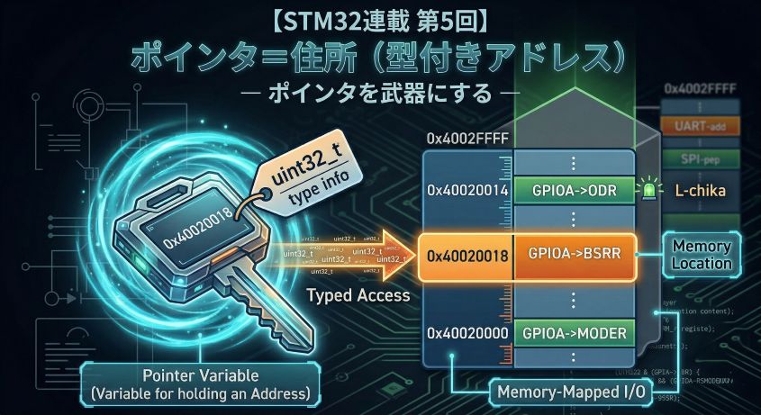
GPIOA register set (base address 0x40020000)

Address        Register   Role
0x40020000    MODER       Pin mode setting
0x40020004    OTYPER      Output type setting
0x40020008    OSPEEDR     Output speed setting
0x4002000C    PUPDR       Pull-up/down setting
0x40020010    IDR         Input data (read pin state)
0x40020014    ODR         Output data (pin ON/OFF)
0x40020018    BSRR        Bit Set/Reset  ← the star of this episode
Both ODR and BSRR are means to “ON/OFF pins,” but their approach differs — which is what we explain now.
STM32 has a dedicated register that solves this problem at the root: BSRR (Bit Set/Reset Register).
The BSRR idea is simple:
Just write “which pin number to turn ON” and “which pin number to turn OFF” in their respective locations
BSRR splits its 32 bits into upper and lower halves:
BSRR register (32 bits)

 Upper half (bit31–bit16)       Lower half (bit15–bit0)
┌──────────────────────┬─────────────────────┐
│ BR15 BR14 ... BR1 BR0 │ BS15 BS14 ... BS1 BS0 │
│     Set LOW            │     Set HIGH          │
└──────────────────────┴─────────────────────┘

BR = Bit Reset (set pin LOW)
BS = Bit Set   (set pin HIGH)
- Writing
1to a bit in the lower half (bits 0–15) sets that pin number HIGH (ON) - Writing
1to a bit in the upper half (bits 16–31) sets that pin number LOW (OFF)
“You don’t need to read the current state.” “No computation needed.” “Just write.” — So there’s no window for an interrupt to interrupt.
An operation that “completes in a single write and cannot be split midway” is called atomic. This is a keyword that appears frequently when studying RTOS (real-time OS) and complex interrupt control — learning it here is a good foundation.
Why is the upper half for Reset? Because 32 bits in one write can simultaneously specify “which pins to turn ON” and “which pins to turn OFF.” For example:
GPIOA->BSRR = (1UL << 0) | (1UL << (1 + 16));sets PA0 HIGH while setting PA1 LOW in a single instruction. Doing the same with ODR would require 2 separate RMW operations, with a risk of state mismatch between them.
4-3. How to Write It
Using PA5 (pin 5) as an example:
// Set PA5 HIGH (LED ON)
// → write 1 to bit5 in the lower half
GPIOA->BSRR = (1UL << 5);          // 0x00000020

// Set PA5 LOW (LED OFF)
// → write 1 to bit5 in the upper half (= 5+16 = bit21)
GPIOA->BSRR = (1UL << (5 + 16));   // 0x00200000
Compared side-by-side with ODR, the simplicity stands out:
// ODR version (requires a read)
GPIOA->ODR |=  (1UL << 5);   // PA5 HIGH ← read→compute→write
GPIOA->ODR &= ~(1UL << 5);   // PA5 LOW  ← read→compute→write

// BSRR version (just write)
GPIOA->BSRR = (1UL << 5);          // PA5 HIGH ← write only
GPIOA->BSRR = (1UL << (5 + 16));   // PA5 LOW  ← write only
“I checked BSRR in the debugger and it shows 0…” BSRR is a write-only register. Values written to it are immediately processed by hardware and reading it always returns
0x00000000. This is expected hardware behavior — it doesn’t mean the write failed. To check the current pin output state, read ODR instead.
4-4. When ODR Is Still Needed
BSRR might seem to make ODR obsolete, but there are 3 things only ODR can do.
① Reading the current output state
Since BSRR is write-only, you must read ODR to know “is PA5 currently HIGH or LOW?”:
// Check PA5's current output state
if (GPIOA->ODR & (1UL << 5)) {
    // PA5 is currently HIGH
} else {
    // PA5 is currently LOW
}
② Toggling a pin
“Flip to the opposite of current state” requires reading the current value. An XOR (^=) RMW on ODR is needed:
// Toggle PA5 (if ON → OFF, if OFF → ON)
GPIOA->ODR ^= (1UL << 5);
BSRR requires specifying “set HIGH” or “set LOW” explicitly, so it’s not suited for toggling.
③ Setting all pins at once
For initialization like “set all GPIOA pins to this state,” writing directly to ODR is simpler:
// Set all pins LOW at once
GPIOA->ODR = 0x0000;
Summary: When to Use Which
| Operation | Register to Use |
|---|---|
| Turn a pin ON | BSRR (BS) |
| Turn a pin OFF | BSRR (BR) |
| Check current output state | ODR (read) |
| Toggle a pin | ODR (^=) |
| Set all pins at once | ODR (direct write) |
Normal ON/OFF operations: use BSRR. ODR is for “when you need to read” or “when you need to toggle.”
4-5. How Other Microcontrollers Handle This
BSRR-style dedicated registers aren’t STM32’s invention alone — but they’re not universal either.
AVR (Arduino’s core)
Arduino’s AVR microcontroller has no equivalent to BSRR. Pin control is done by RMW on the PORT register:
// AVR style (similar to Arduino's digitalWrite internals)
PORTB |=  (1 << PB5);   // HIGH ← read→compute→write (RMW)
PORTB &= ~(1 << PB5);   // LOW  ← read→compute→write (RMW)
This is one reason why BSRR looks elegant to developers coming from Arduino to STM32.
PIC Microcontrollers
PIC uses LAT (Latch) registers, also primarily RMW-based. Only some series have dedicated SET/CLEAR registers.
ESP32 / RP2040 (Raspberry Pi Pico)
Modern popular microcontrollers share the same philosophy as STM32:
| MCU | SET Register | CLEAR Register |
|---|---|---|
| STM32 | BSRR (lower half) | BSRR (upper half) |
| ESP32 | GPIO_OUT_W1TS_REG |
GPIO_OUT_W1TC_REG |
| RP2040 | SIO_GPIO_OUT_SET |
SIO_GPIO_OUT_CLR |
The names differ but the philosophy — “just write to SET/CLEAR” — is the same. This design is becoming standard in the embedded world.
Why doesn’t AVR have it? AVR was designed in the 1990s as an 8-bit architecture, when RMW was considered sufficient. As 32-bit, high-speed clock, and multitasking environments became common, demand for atomic operations grew, and designs like BSRR became prioritized.
Column: Why We Don’t Use Bit Fields
After learning about structs in Episode 3, you might wonder:
“Could I use
struct { uint32_t pin0:1; pin1:1; ... }bit fields for more intuitiveGPIOA->ODR.pin0 = 1;syntax?”
A smart thought, but there are 2 reasons bit fields are avoided in real register operations:
① Lack of atomicity
The GPIOA->ODR.pin0 = 1; assignment still generates RMW assembly. You can’t leverage the hardware advantage of “complete in one write” like BSRR.
② Bit layout is compiler-dependent
The C standard doesn’t specify whether bit fields pack from the right or left — it’s compiler-dependent. Hardware register layouts are strictly defined by the datasheet, so compiler-dependent structs can’t be used safely.
This is why “mask/shift + BSRR” is mainstream in embedded practice. The mask operations that looked unreadable turn out to be the proper craft for safe, reliable hardware manipulation.
✅ Chapter 4 Checklist
- Can explain the roles of BSRR’s upper and lower halves
- Can write the BSRR code to set PA0 HIGH
- Can explain the “step count difference” between ODR and BSRR versions
5. Practice: Experience LED Blinking Three Ways
First, experience directly modifying registers from the debugger without writing any code. Then translate that into code, and finally compare with HAL. Understand in one session how the same LED behavior maps to different implementations.
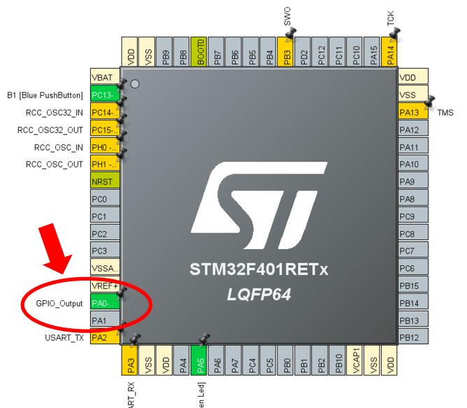
About using PA5 vs PA0 In this practice section we use PA0 (external LED). Chapters 1–2 used PA5 as an example for explanation purposes, but PA5 is connected to the onboard LED (LD2) on the NUCLEO-F401RE. To try with the onboard LED without an external LED, replace
PA0withPA5,(1UL << 0)with(1UL << 5), and(1UL << (0 + 16))with(1UL << (5 + 16)).
5-1. Setup: Circuit and Project
Circuit Wiring
Connect an external LED to PA0. You can access it from the NUCLEO-F401RE Arduino connector (A0 terminal).
LED polarity LEDs have polarity. Connect the anode (longer leg) to the resistor side, cathode (shorter leg) to GND. Reversed insertion won’t light up.
CubeMX Settings
Create a new project in CubeMX or CubeIDE with these settings:
- Set PA0 to GPIO_Output (Pinout & Configuration → PA0 → GPIO_Output)
- Leave clock at default (HSI)
- Generate code
The generated MX_GPIO_Init() handles PA0 output mode setup. We’ll use that initialization as-is and only implement the LED ON/OFF ourselves.
5-2. First: Blink the LED by Writing Registers Directly from the Debugger (No Code!)
Without writing a single line of code, you can make the LED light up by typing values directly into registers in the debugger. This experiment lets you physically feel that “registers are just memory addresses.”
Steps
① Build any code, flash it, and start debugging
Any code with HAL_Delay() in while(1) works. Use Suspend (pause) to stop at any point.
② Open the SFR view
Window → Show View → SFRs
③ Find GPIOA → ODR and type a value directly
| What to do | Value to enter in ODR | Effect |
|---|---|---|
| Turn LED ON | 0x00000001 |
Sets bit0 to 1 → PA0 HIGH → LED lights |
| Turn LED OFF | 0x00000000 |
Clears bit0 to 0 → PA0 LOW → LED off |
Double-click the ODR field in the SFR view, type the value, and the LED lights the moment you press Enter.
The moment you feel “addresses are reality” The LED is under control without writing a single line of code. Just the debugger performing “write 0x00000001 to address 0x40020014” — and the hardware responds instantly. You experience firsthand that registers are just memory addresses, and writing to them from anywhere has the same effect.
To try the same with BSRR
BSRR is Write-Only, so the SFR view may not allow editing. In that case, use the Expressions view:
Window → Show View → Expressions
Add (uint32_t*)0x40020018 and type 0x00000001 (LED ON) or 0x00010000 (LED OFF) in the Value field.
5-3. Writing It as Code
Translate what we did manually in the debugger directly into code.
Register Direct Access Version (using BSRR)
int main(void)
{
    HAL_Init();
    SystemClock_Config();
    MX_GPIO_Init();   // Set PA0 to output mode (leave to HAL)

    while (1)
    {
        // LED ON: set BSRR bit0 (BS0) → PA0 HIGH
        GPIOA->BSRR = (1UL << 0);
        HAL_Delay(500);

        // LED OFF: set BSRR bit16 (BR0) → PA0 LOW
        GPIOA->BSRR = (1UL << (0 + 16));
        HAL_Delay(500);
    }
}
The values we typed manually in the debugger (0x00000001, 0x00010000) appear directly in the code. 1UL << 0 = 0x00000001, 1UL << 16 = 0x00010000 — confirm that debugger operations and code are in one-to-one correspondence.
“PA0 uses
<< 0?” Bit numbers start at 0. PA0 is pin 0, so it’s bit0, PA1 is bit1, PA5 is bit5.1UL << 0is the same as1ULitself, but writing it this way makes the “PA0 → 0 bit shift” mapping explicit.
To monitor the ODR value while the program runs without stopping it, add to Live Expressions:
(uint32_t*)0x40020014
How to add:
- Select Window → Show View → Live Expressions
- Click Add new expression
- Enter
(uint32_t*)0x40020014
While the blink runs, you can watch ODR toggle between 0x00000001 ↔ 0x00000000 in real time. BSRR itself is Write-Only, so monitoring it always shows 0x00000000.
5-4. The HAL Version (for Comparison)
The same LED blink in HAL:
while (1)
{
    // HAL LED ON
    HAL_GPIO_WritePin(GPIOA, GPIO_PIN_0, GPIO_PIN_SET);
    HAL_Delay(500);

    // HAL LED OFF
    HAL_GPIO_WritePin(GPIOA, GPIO_PIN_0, GPIO_PIN_RESET);
    HAL_Delay(500);
}
Looks cleaner, but what’s happening internally?
HAL Internal Implementation (from stm32f4xx_hal_gpio.c)
void HAL_GPIO_WritePin(GPIO_TypeDef* GPIOx, uint16_t GPIO_Pin, GPIO_PinState PinState)
{
    if (PinState != GPIO_PIN_RESET)
    {
        GPIOx->BSRR = (uint32_t)GPIO_Pin;           // SET: write to BS
    }
    else
    {
        GPIOx->BSRR = (uint32_t)GPIO_Pin << 16U;    // RESET: write to BR
    }
}
HAL also uses BSRR internally. What we wrote in the register version is exactly the same operation.
Comparison of Three Implementations
| Approach | Code | Actual Operation |
|---|---|---|
| Debugger direct | None (manual input) | Write 0x00000001 to address 0x40020018 |
| Register direct | GPIOA->BSRR = (1UL << 0) |
Same as above |
| HAL function | HAL_GPIO_WritePin(GPIOA, GPIO_PIN_0, GPIO_PIN_SET) |
Same (internally writes to BSRR) |
All three perform the same write to the same register. Only the abstraction level differs.
Speed Comparison
Is HAL slow? Let’s measure. Using DWT CYCCNT (CPU cycle counter), we can count clock cycles for one LED ON/OFF cycle (DWT is covered in detail in Episode 7):
// Measurement macros
#define DWT_CYCCNT  (*(volatile uint32_t*)0xE0001004)
#define DWT_CTRL    (*(volatile uint32_t*)0xE0001000)

// Enable DWT
DWT_CTRL |= 1;

uint32_t t1, t2, t3, t4, ta, tb;
ta = 0; tb = 0;

// Measure register direct version
t1 = DWT_CYCCNT;
GPIOA->BSRR = (1UL << 0);
t2 = DWT_CYCCNT;
ta = t2 - t1;   // → measured: 11 cycles

// Measure HAL version
t3 = DWT_CYCCNT;
HAL_GPIO_WritePin(GPIOA, GPIO_PIN_0, GPIO_PIN_SET);
t4 = DWT_CYCCNT;
tb = t4 - t3;   // → measured: 40 cycles (function call/branch overhead)
Checking in the Variables view, we get ta = 11, tb = 40:
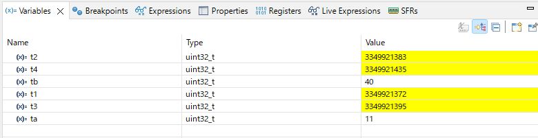
| Implementation | Cycles (measured) | Notes |
|---|---|---|
| Register direct | 11 cycles | Single instruction |
| HAL function | 40 cycles | Function call and branch overhead |
Why Does HAL Take 40 Cycles?
Recall the HAL internal code:
void HAL_GPIO_WritePin(GPIO_TypeDef* GPIOx, uint16_t GPIO_Pin, GPIO_PinState PinState)
{
    if (PinState != GPIO_PIN_RESET)     // ← ② compare and branch
    {
        GPIOx->BSRR = (uint32_t)GPIO_Pin;
    }
    else
    {
        GPIOx->BSRR = (uint32_t)GPIO_Pin << 16U;
    }
}
The 29-cycle overhead comes from:
| Factor | Content |
|---|---|
| ① Function call | BL (Branch with Link) to enter function, BX LR to return — costs several cycles |
| ② Argument setup | Load all 3 arguments (GPIOx, GPIO_Pin, PinState) into registers before calling |
| ③ Branch | The PinState != GPIO_PIN_RESET comparison and conditional branch |
| ④ Stack operations | Save/restore registers on function entry/exit (prologue: stack setup, epilogue: restore) |
Effect of optimization level These measurements are from a debug build with no optimization (
-O0). With optimization enabled (-O2), the compiler may inlineHAL_GPIO_WritePin, generating code equivalent to direct register access. “HAL is slow” is more precisely “HAL is slow in unoptimized debug builds.”
At 84 MHz, 1 cycle ≈ 12 ns. 11 cycles ≈ 130 ns, 40 cycles ≈ 476 ns — a difference of ~350 ns. For LED blinking, this doesn’t matter at all. But in high-speed SPI communication or strict timing control, this difference accumulates into a problem.
Which should you use? For development where readability and maintainability matter, HAL is fine. The practical approach is to use register direct access only in timing-critical sections. The important thing is “knowing what’s happening inside HAL.”
✅ Chapter 5 Checklist
- Wrote a value to BSRR via the debugger SFR view and lit the LED
- Confirmed that register direct and HAL versions “do the same thing”
- Can explain that HAL functions use BSRR internally
- Can explain the speed difference between register direct vs HAL and when to use each
6. Advanced: How RCC Clock Enable Works
6-1. Why Clock Enable Is Needed
In STM32, to save power, peripheral clock supply is stopped by default. Before using GPIOA, you must enable the clock via the RCC (Reset and Clock Control) register.
__HAL_RCC_GPIOA_CLK_ENABLE() in MX_GPIO_Init() serves this purpose.
6-2. Reading the RCC Bit Operation
The actual operation behind __HAL_RCC_GPIOA_CLK_ENABLE() is:
// HAL macro expansion (simplified)
RCC->AHB1ENR |= RCC_AHB1ENR_GPIOAEN;
RCC_AHB1ENR_GPIOAEN is defined as (1UL << 0) — setting bit0 of the AHB1ENR register to 1:
AHB1ENR register (excerpt)
bit7   bit6   bit5   bit4   bit3   bit2   bit1   bit0
GPIOH  GPIOG  GPIOF  GPIOE  GPIOD  GPIOC  GPIOB  GPIOA
                                                    ↑ set this to 1
Without enabling the clock, writes to GPIOA are ignored (or may cause a HardFault — the CPU exception for detecting illegal memory access), and pins won’t respond.
Experiment: what happens if you skip clock enable? Comment out
__HAL_RCC_GPIOA_CLK_ENABLE()and run. Either the LED won’t light at all, or checkingGPIOA->MODERin the debugger shows it doesn’t change (writes don’t reach because the clock is stopped). “Learning by breaking code” in action.
7. Frequently Asked Questions (FAQ)
Q1. Why write 0x3UL? Isn’t 3 enough?
A: A plain 3 is type int (32-bit signed integer). The UL (unsigned long) suffix prevents sign bit manipulation and type mismatch undefined behavior in shift operations. Especially important for shifts at or beyond 32 bits.
Q2. BSRR is write-only — what happens if you read it?
A: Reading BSRR always returns 0x00000000. This is hardware-defined behavior. To check current pin output state, read ODR.
Q3. Does HAL_GPIO_TogglePin() use BSRR internally?
A: HAL_GPIO_TogglePin() reads ODR internally and toggles with XOR — an RMW operation. In scenarios where interrupt contention is a concern, explicit set/clear via BSRR is safer.
// HAL_GPIO_TogglePin internals (simplified)
uint32_t odr = GPIOx->ODR;
GPIOx->BSRR = ((odr & GPIO_Pin) << 16U) | (~odr & GPIO_Pin);
// ↑ actually, even HAL ultimately uses BSRR (depends on HAL version)
Q4. Is leaving GPIO_InitStruct.Speed at LOW OK?
A: For LED blinking, no problem. The Speed setting determines the signal slew rate (how fast LOW→HIGH or HIGH→LOW transitions happen). High-speed SPI communication requires HIGH, but LED blinking is fine with LOW (~2 MHz slew rate). Higher speed settings increase noise radiation, so don’t set higher than needed — that’s professional practice.
Q5. Can I use the same approach with other GPIO ports (GPIOB, GPIOC)?
A: Yes, the structure is identical. However, each requires its own clock enable (__HAL_RCC_GPIOB_CLK_ENABLE(), etc.) and has different addresses:
| Port | Base Address |
|---|---|
| GPIOA | 0x40020000 |
| GPIOB | 0x40020400 |
| GPIOC | 0x40020800 |
| GPIOD | 0x40020C00 |
Episode 4 Summary
This episode covered the craft of register operations and the BSRR philosophy.
What We Learned
✅ Registers = bit collections: Read a 32-bit value as “a collection of configuration switches”
✅ Shift operations: 1UL << n to identify the nth bit
✅ Mask operations: &=~ to clear, |= to set, ^= to toggle
✅ RMW problem: Read-Modify-Write’s 3 steps can be interrupted, causing conflicts
✅ BSRR philosophy: Write-only atomic operation that fundamentally eliminates the RMW problem
✅ Hands-on LED blink: Blinked an LED with BSRR register direct access
Next Steps
Having mastered bit manipulation craft, it’s time to dive into the true nature of pointers.
Many people find pointers intimidating, but it’s the same as what we learned today.
*(uint32_t*)0x40020018 = (1UL << 5); // write directly to BSRR
This code uses pointer-based register access. Understanding pointers as “addresses with types” will make this code immediately readable at a glance.
📖 Previous Episode
📚 Next Episode
Episode 5: "Pointers = Addresses with Types"
Pointers are just addresses with type information. Decode CMSIS headers, GPIO_TypeDef, and the -> operator.
📍 Series Index