This episode uses STM32CubeIDE’s debug features to observe — as concrete numeric values (addresses) — how the microcontroller’s internal state changes as a program executes. Understanding the physical “address” coordinates that underlie C syntax is the goal of this phase.
In Episode 0, we established that embedded programming is a world of “place” (memory) and “time” (execution timing). This time, we’ll use the debugger to actually look at that “place.”
📖 Previous Episode
📘 Next Episode
📍 Series Index
✅ What You'll Be Able to Do After This Episode
- Launch the STM32CubeIDE debugger and operate step execution and breakpoints
- Confirm with the debugger that the program counter (PC) points to a Flash memory address
- Explain the structure of the STM32F401 memory map (Flash / SRAM / peripheral registers)
- Observe GPIO registers in real time using the SFRs view
- Write values directly to GPIO registers from the debugger to toggle an LED
Table of Contents
- Debugger Basics — What a Debugger Does
- Locating Yourself — The Program Counter
- The Address Space Structure — Memory Map
- Hands-On: Enabling Hardware by Writing to Registers
- Hands-On: Watching a Variable Update in SRAM
- Practical Debugging Tips
- FAQ
- Episode 1 Summary
1. Debugger Basics — What a Debugger Does
1-1. Why Do We Need a Debugger?
In PC programming, you use printf() or console.log() to inspect program state. But a microcontroller has no screen and no console.
That’s where the debugger comes in. A debugger pauses program execution and visualizes the CPU’s internal state at that exact moment — register values, memory contents.
With STM32, a hardware debugger called ST-Link is built into the development board, giving your PC real-time visibility into the microcontroller’s internals. No extra hardware needed.
1-2. How the Debugger Works
The debugger communicates through the CPU’s dedicated JTAG or SWD (Serial Wire Debug) interface to:
- Pause execution (breakpoint)
- Read CPU internal registers (PC, SP, general-purpose registers, etc.)
- Read and write memory contents (Flash, SRAM)
- Execute one instruction at a time (step execution)
JTAG / SWD:
These are hardware interfaces for monitoring internal state while a program runs. By connecting to specific pins on the microcontroller, tools like ST-Link get direct access to the chip’s “nervous system.”
1-3. Basic Debug Operations
To monitor the microcontroller’s internal state in real time, you first need to know the step execution controls in STM32CubeIDE.

-
Step Over (F6)
Execute one line at a time. When a function call is encountered, run the whole function without stepping into its internals — only see the result.
Example:HAL_Delay(1000)— you don’t trace inside HAL_Delay; you just wait 1 second and move on. -
Step Into (F5)
Trace inside a function to follow its internal processing.
Use this when you want to see howHAL_GPIO_WritePin()writes to registers internally.
Note: HAL internals are complex — Step Over is sufficient when you’re starting out. -
Breakpoint + Resume (F8)
Double-click the left margin next to a source line to set a breakpoint.
Resume (F8) runs continuously until the next breakpoint.
Great for observing a specific variable change inside a loop — you can watchcounterincrement one step at a time through awhile(1)loop.
Debugging tip:
Start with Step Over (F6) to follow the overall flow, then Step Into (F5) for functions you want to inspect closely.
2. Locating Yourself — The Program Counter
2-1. What Is the Program Counter?
The Program Counter (PC) is a special register that records “which address the CPU is currently executing.”
When you write a C program, the compiler converts it into machine code (binary instructions) stored in Flash memory. The CPU reads one binary instruction from the address the PC points to, executes it, updates the PC, and moves to the next instruction — repeating indefinitely.
1. Read instruction from the address PC points to (Fetch)
2. Decode the instruction (Decode)
3. Execute the instruction (Execute)
4. Update PC to next instruction
5. Go to 1
This is called the fetch-decode-execute cycle — the fundamental operation of every CPU.
2-2. Watching the PC in Action
Start debugging and step through instructions, observing how the CPU’s “current position” moves.
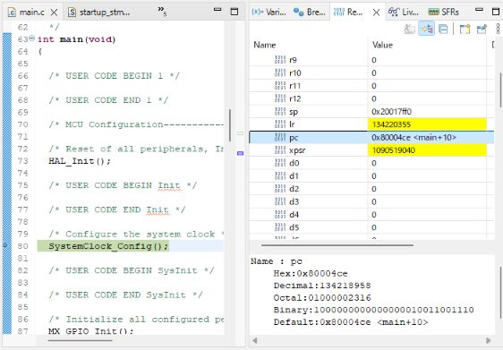
Explanation: Look for the
pcentry in the STM32CubeIDE Registers view. In this example it shows0x80004ce. This is the physical address in Flash memory where the currently executing instruction is stored.
2-3. Reading Hex Addresses
Let’s read 0x80004ce:
- 0x — the prefix meaning “this is hexadecimal”
- 08 — indicates this is in the Flash region (more on that next section)
- 0004ce — the offset within Flash
Hexadecimal uses digits 0–9 and letters A–F. One digit represents 0–15, making large numbers like memory addresses compact.
| Decimal | Hex | Binary |
|---|---|---|
| 0 | 0x0 | 0000 |
| 10 | 0xA | 1010 |
| 15 | 0xF | 1111 |
| 255 | 0xFF | 11111111 |
| 2316 | 0x4ce | 010011001110 |
Why hexadecimal?
Computers work in binary, but binary has too many digits to read. One hex digit represents exactly four binary bits — making hex both human-readable and directly aligned to how computers work.
2-4. The CPU as a State Machine
The CPU reads binary instructions from the address the PC points to, executes them, updates the PC, and repeats — it’s a state machine.
For example:
int main(void) {
    int counter = 0;        // instruction at address 0x08000500
    counter++;              // instruction at address 0x08000504
    HAL_GPIO_WritePin(...); // instruction at address 0x08000508
}
The compiler converts this to machine code and writes it to Flash. Step through with the debugger and watch PC advance: 0x08000500 → 0x08000504 → 0x08000508.
3. The Address Space Structure — Memory Map
3-1. Everything Is Managed by Addresses
Every resource in a microcontroller (memory, peripherals) is placed in a single address space. Think of it like a city’s addressing system.
Just as Tokyo has districts (Chiyoda, Shinjuku, Shibuya), a microcontroller’s address space has regions: “Flash region,” “SRAM region,” “Peripheral register region.”
3-2. STM32 Memory Map
| Address Range | Physical Region | Primary Role | Size Example (STM32F4) |
|---|---|---|---|
| 0x0800 0000 onward | Flash | Stores program instructions (read-only) | 512 KB – 2 MB |
| 0x2000 0000 onward | SRAM | Holds dynamic data — variables | 64 KB – 512 KB |
| 0x4000 0000 onward | Peripheral registers | Hardware configuration interface (GPIO, comms, timers) | (varies by peripheral) |
Flash vs SRAM:
- Flash: Non-volatile — content survives power off. Stores program code and constant data. Limited write cycles; read speed is fast.
- SRAM: Volatile — content is lost at power off. Stores variables and temporary data. Very fast read/write, no write cycle limit.
3-3. Memory-Mapped I/O
Controlling hardware through memory operations is called Memory-Mapped I/O.
For example, GPIOA’s data output register is at address 0x40020014. Writing a value to this address changes the physical voltage on a pin.
// Write 0x0020 to address 0x40020014
*(uint32_t*)0x40020014 = 0x0020;
// → GPIOA pin 5 goes HIGH (LED on, etc.)
Think of it as pressing a “switch” at a specific address. Send data to that address and the hardware responds.
3-4. Why Use Addresses for Everything?
Managing everything through “addresses” simplifies CPU design. The CPU only needs two basic operations: “read data from memory” and “write data to memory.” With these two operations, it can control all hardware.
This means loading program instructions, updating variables, and controlling hardware are all achieved with the same instruction set.
4. Hands-On: Enabling Hardware by Writing to Registers
4-1. What Is a Register?
The word “register” appears constantly in embedded programming, and it has two meanings depending on context:
- CPU registers: Ultra-fast temporary storage inside the CPU (R0, R1, PC, SP, etc.)
- Peripheral registers: Specific memory addresses that manage settings and state for peripherals (GPIO, UART, timers, etc.)
Here we focus on peripheral registers.
Peripheral registers are “configuration windows” at specific memory addresses. Write a value to those addresses and you control hardware behavior.
4-2. GPIO Register Types
For GPIOA (General Purpose I/O port A), the relevant registers are:
| Register | Address | Role |
|---|---|---|
| MODER | 0x40020000 | Pin mode (input / output / alternate function / analog) |
| OTYPER | 0x40020004 | Output type (push-pull / open-drain) |
| OSPEEDR | 0x40020008 | Output speed |
| PUPDR | 0x4002000C | Pull-up / pull-down |
| ODR | 0x40020014 | Output data register (pin HIGH / LOW) |
| IDR | 0x40020010 | Input data register (read pin state) |
Writing the right values to these registers sets a pin to “output mode” or toggles it HIGH/LOW.
4-3. Running an Initialization Function
Execute MX_GPIO_Init() with Step Over (F6) and watch the peripheral register values change.
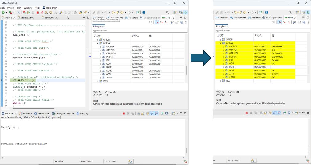
Explanation: When the function runs, configuration values are written to the GPIOA registers near base address
0x40020000. These writes physically determine hardware state — the specific pin is now in “output mode.” You can see values becoming defined and highlighted in yellow.
4-4. What Is Happening Inside?
Inside MX_GPIO_Init(), something like this occurs:
// Enable GPIOA clock (power it on)
RCC->AHB1ENR |= RCC_AHB1ENR_GPIOAEN;

// Set PA5 to output mode
GPIOA->MODER &= ~(0x3 << (5 * 2));  // clear existing setting
GPIOA->MODER |= (0x1 << (5 * 2));   // 01 = output mode

// Set PA5 to push-pull output
GPIOA->OTYPER &= ~(0x1 << 5);       // 0 = push-pull

// Set PA5 to low-speed output
GPIOA->OSPEEDR &= ~(0x3 << (5 * 2)); // 00 = low speed
Every one of these operations is “write a specific value to a specific address.” In other words, hardware configuration is done through memory writes.
5. Hands-On: Watching a Variable Update in SRAM
5-1. Where Does a Variable Live?
Next, update variable counter inside a while(1) loop and watch a specific SRAM address change. Set a breakpoint on counter++ and use F8 (Resume) to stop there repeatedly.
int main(void) {
    HAL_Init();
    SystemClock_Config();
    MX_GPIO_Init();

    uint32_t counter = 0;  // 32-bit unsigned integer (4 bytes)

    while(1) {
        counter++;         // ← set breakpoint here
        HAL_Delay(1000);
    }
}
5-2. Watching the Variable Change
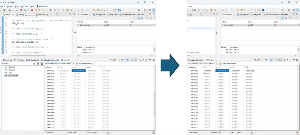
Explanation: Variable
counteris located at SRAM address0x20017FF4.Left (initial state): Right after program start,
counter = 0. Variables view shows0; Memory view at0x20017FF4shows raw bytes00 00 00 00.Right (after 10 loop iterations): After stopping at the breakpoint 10 times,
counter = 10. Variables view shows10; Memory view shows0A 00 00 00at the same address. (0Ain hex is decimal10.)
This is the core insight: a C variable’s value change is directly observable in the debugger as a byte-level change at a specific physical memory address.
5-3. Little-Endian Byte Order
Notice that value 10 is stored in memory as 0A 00 00 00.
uint32_t is a 32-bit (4-byte) integer. The number 10 in 32-bit hex is:
Decimal:  10
Binary:   00000000 00000000 00000000 00001010
Hex:      0x0000000A
Split into 4 bytes:
| Byte position | Hex | Decimal |
|---|---|---|
| Least significant byte | 0x0A | 10 |
| 2nd byte | 0x00 | 0 |
| 3rd byte | 0x00 | 0 |
| Most significant byte | 0x00 | 0 |
STM32 (ARM architecture) uses little-endian byte order — the least significant byte is stored at the lowest address.
So in memory:
| Address | Value stored |
|---|---|
| 0x20017FF4 | 0x0A (least significant byte) |
| 0x20017FF5 | 0x00 |
| 0x20017FF6 | 0x00 |
| 0x20017FF7 | 0x00 (most significant byte) |
The Memory view shows these consecutively as 0A 00 00 00.
Little-endian vs Big-endian:
- Little-endian: least significant byte at lowest address (STM32, x86, etc.)
- Big-endian: most significant byte at lowest address (some network equipment)
Neither is better — they just need to agree when exchanging data.
5-4. The Essence of Variable Operations
In embedded programming, “operating on a variable” is nothing more than a physical phenomenon: the CPU updating a bit pattern stored at a specific memory address.
The C statement counter++ compiles to roughly:
1. Load value from address 0x20017FF4 (LOAD instruction)
2. Add 1 to that value (ADD instruction)
3. Write result back to address 0x20017FF4 (STORE instruction)
Every high-level language abstraction ultimately reduces to “specify an address and read or write memory.”
6. Practical Debugging Tips
6-1. Opening the Memory View
In STM32CubeIDE, to examine a specific address while paused in debug:
- Window → Show View → Memory
- Click the “+” button in the Memory view
- Enter an address (e.g.,
0x20017FF4) or variable expression (e.g.,&counter) - Press Enter to see the contents
6-2. Using the Registers View
The Registers view shows all CPU and peripheral registers:
- Core Registers: PC, SP, LR, general-purpose registers (R0–R15), etc.
- Peripheral Registers: GPIOA, USART1, TIM2, etc. (project-dependent)
Expand a peripheral to see individual bit fields (MODER, OTYPER, etc.).
6-3. Data Breakpoints (Watchpoints)
A normal breakpoint stops at “when a specific line is reached.” A data breakpoint (watchpoint) stops when “the value at a specific memory address changes.”
How to set:
- Right-click a variable in the Variables view
- Select Add Watchpoint (C/C++)
- The debugger automatically stops when that address changes
This solves “I don’t know where my variable is being overwritten.”
6-4. Expressions View
To continuously monitor specific expressions or variables during a debug session:
- Window → Show View → Expressions
- Click Add new expression (the green + icon)
- Enter an expression (e.g.,
counter * 2,counter > 100)
Registered expressions are automatically evaluated each time execution stops.
Scope limitation:
Expressions view can only evaluate variables in the current scope. Local variables are only available while stopped inside their function. For persistent monitoring, use global orstaticvariables.
6-5. SFRs View (Peripheral Register Monitoring)
For detailed peripheral register monitoring, use the SFR (Special Function Registers) view:
- Window → Show View → SFRs
- Expand a peripheral (e.g., GPIOA, TIM2) to see individual registers and bit fields
- Values update automatically each time execution stops (changes highlighted in yellow)
More readable than the Registers view for bit-level changes.
7. FAQ
Q1. Why separate Flash and SRAM?
A: They have different roles.
- Flash is non-volatile — your program survives power-off. But writes are slow and there’s a write-cycle limit. Reads are fast.
- SRAM is volatile — contents are lost at power-off, but reads and writes are very fast with no write-cycle limit.
Using both efficiently builds better systems.
Q2. How is a variable’s address decided?
A: The compiler and linker decide automatically.
At compile time, the linker assigns addresses based on variable size and placement rules. Global variables get fixed addresses; local variables are dynamically placed on the stack (covered in the next episode).
Q3. Where do I find register addresses?
A: In the Reference Manual provided by ST Microelectronics.
For example, STM32F446 uses “RM0390 Reference Manual” — it documents every peripheral register address and bit definition. Free to download from ST’s website.
Q4. The debugger shows different values than the actual behavior. Why?
A: Compiler optimization is likely the cause.
Debug builds (-O0) disable optimization — variables and memory map 1-to-1. Release builds (-O2, -O3) allow the compiler to store variables in CPU registers or eliminate “unnecessary” operations, breaking the source-to-memory correspondence.
Always use a Debug build configuration when debugging.
Q5. What happens when I access a wrong address?
A: Depends on whether the MCU has memory protection.
- With MPU (Memory Protection Unit): A HardFault exception fires and the program stops.
- Without MPU: Undefined behavior — unexpected values may be read/written, the system may run wild.
Many STM32 series have an MPU — if properly configured, illegal accesses are detected.
Episode 1 Summary
We used the debugger to peek inside the microcontroller’s “address world.” Key points:
-
CPU execution control: PC steps through Flash addresses sequentially. The CPU is a state machine running the fetch-decode-execute cycle.
-
Hardware configuration: Write to peripheral registers at specific addresses to activate circuits. Memory-mapped I/O unifies hardware control under the same paradigm as memory operations.
-
Data management: Variables are numeric values at specific SRAM addresses. Stored in little-endian format — least significant byte first.
Everything is managed through the coordinate system of “addresses.” C language syntax is just an abstraction over those address operations. This is the true nature of embedded systems.
“Variables,” “hardware control,” and “program execution” — all achieved through the single unified operation of “reading and writing specific addresses.”
What You Learned
✅ Basic debugger operations (step over, step into, breakpoints)
✅ The program counter (PC) and the CPU’s instruction execution cycle
✅ Memory map structure (Flash, SRAM, peripheral registers)
✅ Hardware control through peripheral register writes
✅ Variables in SRAM and little-endian byte order
✅ Practical debugging tools (Memory view, Registers view)
What’s Next
Next episode: how the linker organizes all these addresses into named sections (.text, .data, .bss, stack, heap) — and what that means for variable placement.
📍 Series Index