This article contains affiliate links (Amazon Associates).
Why the 74HC595 Is Still the Best GPIO Expander
Every Arduino developer runs out of pins eventually
Build anything non-trivial on an Arduino and you will hit the same wall: “I don’t have enough GPIO pins.”
- You want to connect an LCD (4–8 pins)
- You need several LED indicators
- You’re driving motors and reading sensors at the same time
- And you still want serial communication…
The Arduino UNO R4 is dramatically faster than the R3, but the physical pin count is unchanged. That is where the 74HC595 shift register comes in.
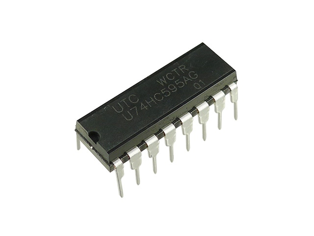
What makes it so compelling
The reasons the 74HC595 remains overwhelmingly popular in 2026 are easy to state:
🚀 Unlimited expansion from three signal lines
- Data (SER): serial data input
- Clock (SRCLK): shift timing
- Latch (RCLK): output update
Those three lines control 8 bits (8 outputs), and cascading extends that without limit.
💰 Unbeatable on cost
- Roughly ¥30–50 each (as of February 2026)
- Minimal assembly cost in volume
- Plenty of second sources, so supply is stable
⚡ Works with high-speed SPI
Arduino’s built-in shiftOut() works fine, but with hardware SPI you get megahertz-class transfer rates — fast enough for LED matrices and multiplexers with real-time requirements.
🔌 Native 5 V operation
Modern I2C devices are increasingly 3.3 V only, whereas the 74HC595 runs across a wide 2 V–6 V range and can be wired directly to an Arduino UNO R4 with no level shifting.
What this project covers
- How to use the 74HC595 and how shift-register/SPI transfer works (with diagrams a beginner can follow)
- Circuit and PCB design in KiCad (design files published)
- Ordering assembled boards from JLCPCB (and how the economics work out)
- Cascading for multi-stage expansion (theoretically unlimited)
- Arduino sample code (published on GitHub)
Quick Start
If you just want it working, here’s the three-step version.
Step 1: Wiring
| 74HC595 pin | Arduino UNO R4 pin | Description |
|---|---|---|
| SER (14) | D11 | Serial data input |
| SRCLK (11) | D13 | Shift clock |
| RCLK (12) | D10 | Latch (output update) |
| OE (13) | GND | Output enable (tie low permanently) |
| SRCLR (10) | 5V | Reset disabled (tie high permanently) |
| VCC (16) | 5V | Power |
| GND (8) | GND | Ground |
| QA–QH (15, 1–7) | To LEDs, etc. | 8-bit output |
Step 2: Sample code (shiftOut)
const int SER  = 11;  // data
const int SRCLK = 13; // clock
const int RCLK = 10;  // latch

void setup() {
  pinMode(SER, OUTPUT);
  pinMode(SRCLK, OUTPUT);
  pinMode(RCLK, OUTPUT);
}

void loop() {
  for (int i = 0; i < 8; i++) {
    digitalWrite(RCLK, LOW);
    shiftOut(SER, SRCLK, MSBFIRST, 1 << i); // light one bit at a time
    digitalWrite(RCLK, HIGH);
    delay(200);
  }
}
Step 3: Verify
Connect an LED through a 220 Ω resistor to each of QA–QH. Upload the sketch above and you should see the LEDs light one after another as the data shifts through.
- Confirm the OE pin (13) is tied to GND — if it stays high the outputs are disabled
- Confirm the SRCLR pin (10) is tied to 5 V — if it stays low the register is held in reset
- Check the RCLK ordering: drive it high after
shiftOut()completes, not before
How the 74HC595 Actually Works
What it is
The 74HC595 is an 8-bit SIPO (Serial In, Parallel Out) shift register.
“Serial in” means data arrives one bit at a time. “Parallel out” means all 8 bits appear simultaneously across 8 output pins.
In other words, think of the 74HC595 as a converter that distributes data arriving on one wire across eight wires. Using it from Arduino is straightforward — no special library is required, since Arduino’s built-in shiftOut() function or the SPI library is all you need, and most beginners have it working within minutes.
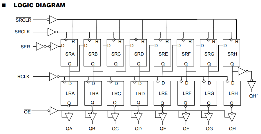
74HC595 internal block diagram
Why “shift” register?
Internally, eight storage elements (flip-flops) sit in a chain. Every clock pulse shifts the data along by one bit.
Clock 1: [1][0][0][0][0][0][0][0]
Clock 2: [0][1][0][0][0][0][0][0]  ← data moves along
Clock 3: [1][0][1][0][0][0][0][0]
...
That shifting behaviour is what lets a single wire fill up eight bits of storage.
Pinout and pin functions
The important pins on the DIP package:
| Pin | Name | Function | Typical Arduino connection |
|---|---|---|---|
| 14 | SER (DS) | Serial data input | D11 (MOSI) |
| 11 | SRCLK (SHCP) | Shift register clock | D13 (SCK) |
| 12 | RCLK (STCP) | Storage register clock (latch) | D10 (SS) |
| 13 | OE | Output enable (active low) | GND (always enabled) |
| 10 | SRCLR | Shift register clear (active low) | +5 V (reset disabled) |
| 9 | QH’ | Serial output for cascading | To the next stage’s SER |
| 15–1, 7 | QA–QH | Parallel output (8 bits) | LEDs, motors, etc. |
The two-stage output update (important)
What sets the 74HC595 apart from simpler shift registers is that it has two stages: a shift register and a storage register.
1. Shift register (internal buffer)
Data arriving on SER is clocked in by SRCLK until eight bits are stored. At this point nothing has changed on the output pins.
2. Storage register (output buffer)
Once all eight bits are in place, toggling RCLK transfers them to the output pins (QA–QH) all at once.
Why the two stages matter
With only one stage, the outputs would change continuously while data was shifting through — causing LEDs to flicker and motors to twitch.
Two stages separate “prepare the data” from “update the output”, giving glitch-free, stable control. This is exactly why professional board designs still reach for the 74HC595.
Timing sequence
The actual signal exchange proceeds like this:
Time  SER  SRCLK  RCLK  → Output (QA-QH)
T0    1     ↑     L     → no change (loading)
T1    0     ↑     L     → no change
...
T7    1     ↑     L     → no change (8 bits now loaded)
T8    -     -     ↑     → all outputs update at once!
Every output changes at the instant RCLK rises. That simultaneous update is the whole point of the part.
Driving it from an Arduino UNO R4
The basic approach is the shiftOut() function:
// Send the value 0b10101010
digitalWrite(latchPin, LOW);           // open the latch
shiftOut(dataPin, clockPin, MSBFIRST, 0b10101010);
digitalWrite(latchPin, HIGH);          // close the latch, updating the outputs
For faster control, use hardware SPI:
#include <SPI.h>

void setup() {
  SPI.begin();
  SPI.setClockDivider(SPI_CLOCK_DIV2);  // faster
}

void loop() {
  digitalWrite(latchPin, LOW);
  SPI.transfer(0b10101010);  // roughly 10x faster than shiftOut()
  digitalWrite(latchPin, HIGH);
}
Full Arduino UNO R4 Compatibility
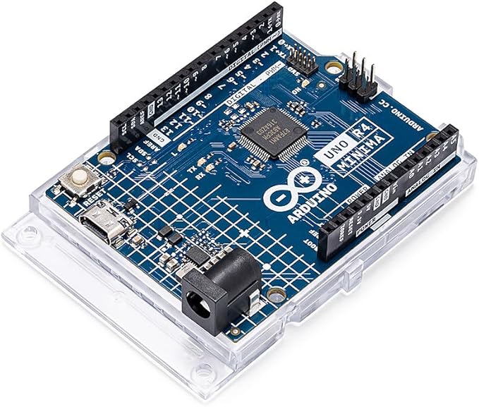
Arduino UNO R4 Minima
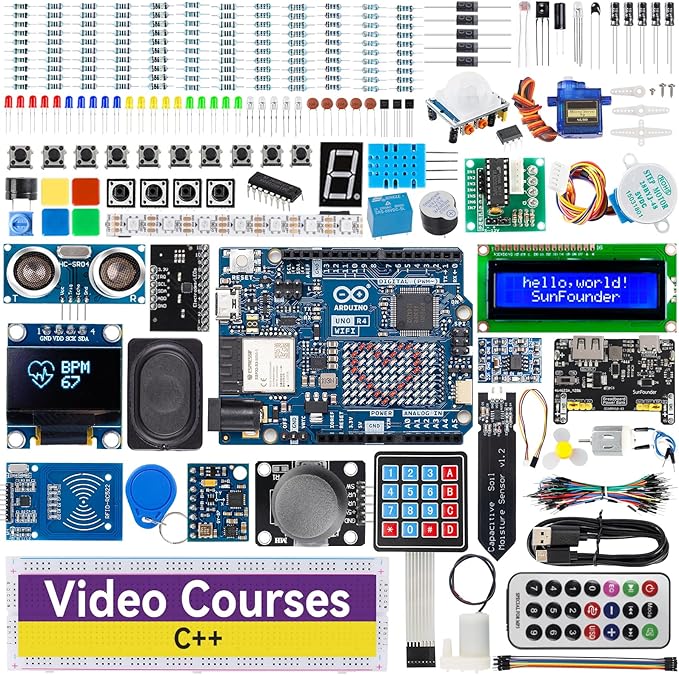
Arduino UNO R4 Minima starter kit
Where the R4’s improvements pay off
| UNO R3 | UNO R4 Minima | Effect on 74HC595 control | |
|---|---|---|---|
| CPU | ATmega328P (8-bit) | RA4M1 (32-bit Cortex-M4) | Enables high-speed SPI |
| Clock | 16 MHz | 48 MHz | 3× the data transfer rate |
| Max SPI speed | 8 MHz | 24 MHz | Less latency when cascading |
| Digital pins | 14 | 14 | Pinout unchanged from R3 |
Important: the R4 is far faster, but the pinout is fully R3-compatible. Everything in this article — schematic and code alike — works on both.
R4-specific gotchas
Fixing USB upload errors
If the R4 Minima throws a “DFU mode” error on the first upload:
- Press the RST button twice, quickly
- When the on-board LED pulses orange, start the upload
- Use Arduino IDE 2.x (the 1.8 series is unreliable here)
Circuit Design
Design goals
The board was designed around three requirements:
- Cascadable: chain multiple boards for unlimited expansion
- Visual debugging: an LED on every bit so state is immediately visible
- Cost-optimised: parts chosen for compatibility with JLCPCB assembly
Walking through the schematic
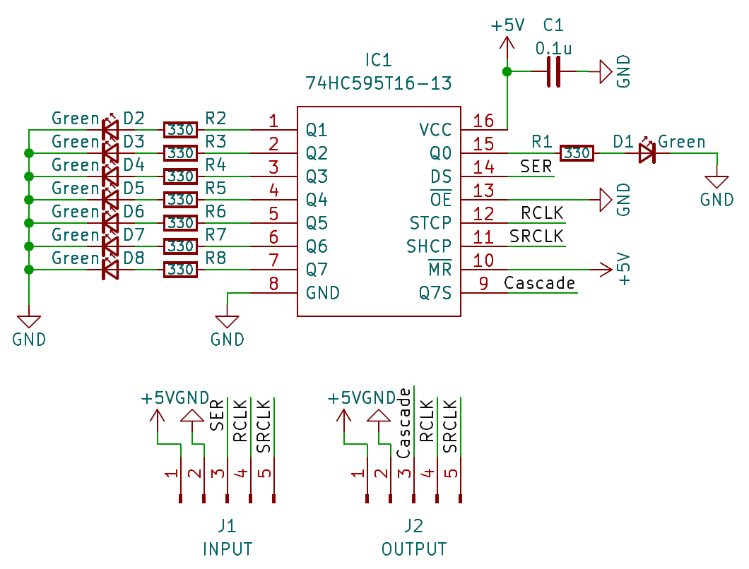
Schematic of the 74HC595 LED control board
Power section
- VCC (5 V) and GND supplied from the Arduino
- A bypass capacitor (0.1 µF) placed right next to the 74HC595’s VCC pin
- Suppresses noise during fast switching
- Compensates for momentary supply droop
74HC595 connections
Arduino           74HC595
D11 (MOSI)  →  SER  (Pin 14)   data input
D13 (SCK)   →  SRCLK (Pin 11)  shift clock
D10 (SS)    →  RCLK (Pin 12)   latch
- OE (Pin 13) → GND: outputs always enabled
- SRCLR (Pin 10) → VCC: reset disabled (pulled up)
- QH’ (Pin 9) → next stage’s SER: for cascading
LED drive section
Each output (QA–QH) drives:
QA (Pin 15) ─┬─ resistor (330Ω) ─ LED (green) ─ GND
             └─ jumper (optional disable)
How the resistor value was chosen:
- 74HC595 output voltage: 5 V
- Green LED forward voltage: Vf = 2.0 V
- Target LED current: 10 mA (a balance of visibility and power draw)
R = (5V - 2.0V) / 10mA = 300Ω
→ nearest E24 value is 330Ω
Actual current: (5V - 2.0V) / 330Ω ≈ 9.1mA
Total current with all 8 lit: about 73 mA — comfortably inside the 74HC595’s 150 mA maximum.
How cascading works
To chain boards, connect QH’ of the first stage to SER of the second.
Arduino → [Board 1] QH' → SER [Board 2] QH' → SER [Board 3] ...
The first 8 bits the Arduino sends end up in board 3, the next 8 in board 2, and the last 8 in board 1.
Control code for three cascaded boards:
digitalWrite(latchPin, LOW);
shiftOut(dataPin, clockPin, MSBFIRST, 0b10101010);  // board 3
shiftOut(dataPin, clockPin, MSBFIRST, 0b11001100);  // board 2
shiftOut(dataPin, clockPin, MSBFIRST, 0b11110000);  // board 1
digitalWrite(latchPin, HIGH);  // all three update simultaneously
PCB layout (designed in KiCad)
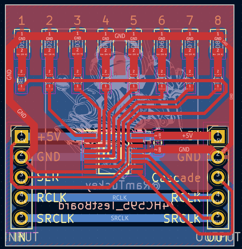
74HC595 LED control board layout
Layout decisions
- Signal routing: SPI lines kept as short as possible to reduce noise
- Ground plane: full copper pour on the back side to stabilise the supply
- Connector placement: pin headers/sockets at the top and bottom edges so boards can stack
- Silkscreen: pin numbers and QA–QH outputs clearly marked
Board specification
- Size: 50 mm × 50 mm (within JLCPCB’s cheapest bracket)
- Layers: 2 (top and bottom)
- Thickness: 1.6 mm (standard)
- Finish: HASL (lead-free)
Ordering Assembled Boards from JLCPCB
Why use the assembly service
Compared to hand-soldering resistors and LEDs across 30 boards (240 parts), JLCPCB’s assembly service wins on time, quality, and cost simultaneously.
| Hand assembly | JLCPCB assembly | |
|---|---|---|
| Sourcing | Buy from local suppliers | Pulled automatically from JLCPCB stock |
| Assembly time | Hours of hand-soldering 240 parts | Zero (machine placed) |
| Quality | Risk of bad joints | Uniform reflow soldering |
| Cost | Parts + your time | About $1.50 per board including the PCB |
Preparing the order files
1. Gerber files (from KiCad)
Use Plot → Gerber Format and output these layers:
- F.Cu, B.Cu (top and bottom copper)
- F.SilkS, B.SilkS (silkscreen)
- F.Mask, B.Mask (solder mask)
- Edge.Cuts (board outline)
- Drill files
→ Zip them together and upload to JLCPCB.
2. BOM file (bill of materials)
Create a CSV in this format:
Comment,Designator,Footprint,LCSC Part #
74HC595D,U1,SOIC-16,C5947
330Ω,R1-R8,0805,C17630
LED Green,D1-D8,0805,C2297
0.1µF,C1,0805,C49678
LCSC Part # is JLCPCB’s stock number — look parts up at LCSC.com to find it.
3. CPL file (component placement)
Generate it in KiCad with Place → Footprint Position File. It’s a CSV listing X/Y coordinates and rotation angles.
The actual order and what it cost
The order placed for this project (February 2026):
- Quantity: 30 boards
- Board size: 50 mm × 50 mm
- Assembly: single side
- Parts per board: 18 (1 IC, 8 resistors, 8 LEDs, 1 capacitor)
Cost breakdown:
PCB fabrication:  $8.50
Assembly:         $18.00 (setup fee)
Components:       $15.20 (for 30 boards)
Shipping:         $12.00 (DHL Express)
──────────────────
Total:            $53.70 (about ¥6,800)
Per board:        about ¥227
Compared with doing it by hand:
- Parts: about ¥5,000 to buy the same components locally
- Labour: about 6 hours of hand-soldering (¥6,000 at ¥1,000/hour)
- ¥11,000 by hand → ¥6,800 with assembly
The quality of what arrived
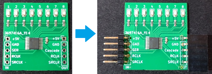
Assembled boards as delivered by JLCPCB
- Resistors, LEDs, and ICs all placed accurately
- Solder fillets uniform across the batch (the advantage of a reflow oven)
- About 7 days from order to delivery (via DHL Express)
What’s left for you to do:
- Solder the through-hole pin headers and sockets
- Verify operation
That’s the real appeal of the assembly service.
Assembly and Cascading
Soldering the through-hole parts
Solder the pin headers and sockets onto the delivered boards.
A board before the connectors are fitted
Recommended parts:
- Pin headers (male): 2.54 mm pitch, straight
- Pin sockets (female): 2.54 mm pitch, stackable
Soldering tips:
- Hold the board firmly in a jig (or a third-hand tool)
- Tack two diagonal pins first, then check the header is square before continuing
- Once it looks right, solder the remaining pins
- Flux makes the solder flow noticeably better
Five boards chained together
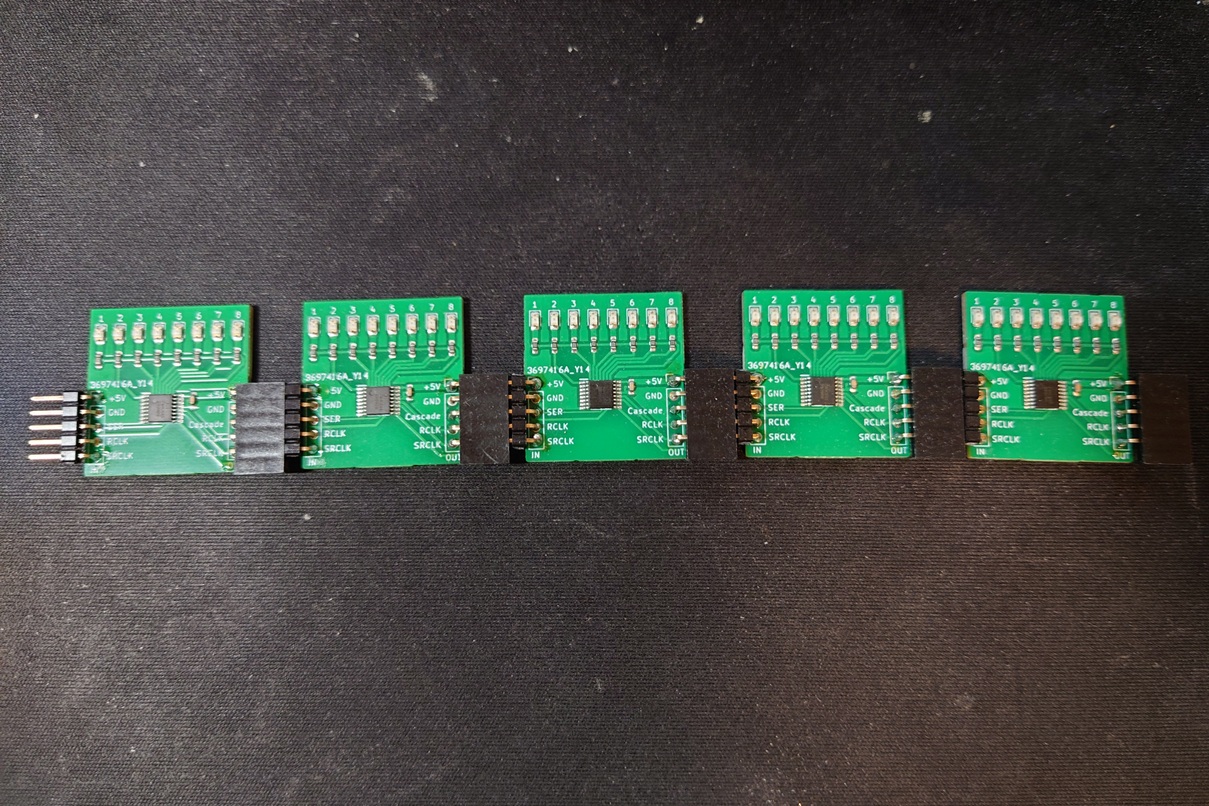
Five 74HC595 boards cascaded
Chaining five boards gives you 40 LEDs driven from just three Arduino pins.
Control code (5 boards = 40 LEDs):
const int latchPin = 10;  // RCLK
const int clockPin = 13;  // SRCLK
const int dataPin = 11;   // SER

void setup() {
  pinMode(latchPin, OUTPUT);
  pinMode(clockPin, OUTPUT);
  pinMode(dataPin, OUTPUT);
}

void loop() {
  // Send 5 bytes, one per board
  digitalWrite(latchPin, LOW);

  shiftOut(dataPin, clockPin, MSBFIRST, 0b10101010); // board 5
  shiftOut(dataPin, clockPin, MSBFIRST, 0b01010101); // board 4
  shiftOut(dataPin, clockPin, MSBFIRST, 0b11110000); // board 3
  shiftOut(dataPin, clockPin, MSBFIRST, 0b00001111); // board 2
  shiftOut(dataPin, clockPin, MSBFIRST, 0b11001100); // board 1

  digitalWrite(latchPin, HIGH);  // all 40 LEDs update at once
  delay(500);
}
Demo video
All the boards light and extinguish in perfect sync. There is no perceptible lag even when cascaded, which demonstrates how much headroom SPI transfer has here.
How far can cascading go?
Q: How many boards can you chain?
In theory there is no limit. In practice, three things constrain it.
1. Signal degradation
The 74HC595’s digital outputs are robust, but at 10 or 20 boards the rise and fall times start to soften.
Mitigations:
- Insert a buffer IC (e.g. 74HC244) every 5–10 boards
- Match the impedance of the signal lines (a 100 Ω series resistor helps)
2. Power delivery
Lighting all of 8 LEDs × 30 boards = 240 LEDs draws:
Current = 9.1mA × 240 = 2.18A
The Arduino’s 5 V pin can supply only about 500 mA, so an external supply is mandatory.
Recommended arrangement:
- Arduino: control signals only
- External 5 V supply (3 A or more): powers the LEDs
- Share the ground between the two, so they reference the same potential
3. Data transfer time
For 100 cascaded boards, sending a complete frame takes:
shiftOut(): 8 bits × 100 boards = 800 bits
Transfer rate: about 250 kbps (using shiftOut())
Time: 800 bits / 250 kbps ≈ 3.2 ms
To refresh at 60 fps you have 16.7 ms per frame, so there is plenty of margin. At the thousand-board level, however, this becomes the bottleneck.
Practical Applications
1. Driving an LED matrix
An 8×8 LED matrix needs only two 74HC595s:
- The first: row select (8 lines)
- The second: column data (8 lines)
Combine that with multiplexed scanning and you drive 64 LEDs from two ICs.
2. Multi-digit seven-segment displays
Ideal for clocks and counters. One 74HC595 drives one digit (8 segments), and cascading adds digits.
[Arduino] → [74HC595] → 7seg (digit 1)
              ↓ QH'
           [74HC595] → 7seg (digit 2)
              ↓ QH'
           [74HC595] → 7seg (digit 3)
3. Relay control (home automation)
To switch multiple appliances, use the 74HC595’s outputs to drive transistors or MOSFETs, which in turn switch relays.
Cautions:
- A relay coil generates back-EMF, so fit a flyback diode (e.g. 1N4007) in parallel with it
- The 74HC595 outputs are limited to 25 mA, so drive the relay through a transistor rather than directly
4. An I2C-to-74HC595 bridge
You might ask why not just use an MCP23017 over I2C. The 74HC595 is cheaper and easier to source, so some people build an adapter board that controls 74HC595s over I2C instead.
Sample Code and Published Resources
Basic blink sketch
// Basic 74HC595 control (works on the Arduino UNO R4)
const int latchPin = 10;  // RCLK (SS)
const int clockPin = 13;  // SRCLK (SCK)
const int dataPin = 11;   // SER (MOSI)

void setup() {
  pinMode(latchPin, OUTPUT);
  pinMode(clockPin, OUTPUT);
  pinMode(dataPin, OUTPUT);
}

void loop() {
  // Light each output in sequence
  for (int i = 0; i < 8; i++) {
    digitalWrite(latchPin, LOW);
    shiftOut(dataPin, clockPin, MSBFIRST, 1 << i);  // bit shift
    digitalWrite(latchPin, HIGH);
    delay(100);
  }
}
Hardware SPI version (faster)
#include <SPI.h>

const int latchPin = 10;

void setup() {
  pinMode(latchPin, OUTPUT);
  SPI.begin();
  SPI.setClockDivider(SPI_CLOCK_DIV2);  // maximum speed (24MHz / 2 = 12MHz)
  SPI.setBitOrder(MSBFIRST);
  SPI.setDataMode(SPI_MODE0);
}

void loop() {
  digitalWrite(latchPin, LOW);
  SPI.transfer(0b10101010);  // about 10x faster than shiftOut()
  digitalWrite(latchPin, HIGH);
  delay(100);
}
Published on GitHub
Everything is available from these links:
-
LED sample program (Arduino sketch) https://github.com/ramtuc/ram_prog/tree/main/74HC595_testboard/Arduino_Schetch
-
KiCad schematic and board data (.kicad_pro, .kicad_sch, .kicad_pcb) https://github.com/ramtuc/ram_prog/tree/main/74HC595_testboard/schematic
Ready-to-use JLCPCB order files
Download 74HC595_testboard.zip and you get:
- Gerber files (for fabrication)
- BOM file (with LCSC part numbers)
- CPL file (component placement coordinates)
Ordering steps:
- Go to the JLCPCB website
- Upload
74HC595_testboard.zip - Enable “PCB Assembly”
- Upload the BOM and CPL files
- Review the placement preview and place the order
A few days later, boards with the LEDs and resistors already fitted arrive at your door.
Troubleshooting
Q1: No LEDs light at all
Things to check:
-
Power
- Is 5 V actually reaching the 74HC595’s VCC pin?
- Do the Arduino and the board share a ground?
-
Wiring mistakes
- Are SER, SRCLK, and RCLK on the right pins?
- Compare the schematic against the physical wiring once more
-
The OE pin (output enable)
- Confirm OE is pulled to GND — if it’s high, the outputs are disabled
-
The SRCLR pin (reset)
- Confirm SRCLR is tied to 5 V — if it’s low, the register is held in reset
Q2: The second and later stages don’t work when cascading
Cause: by far the most common is a missing QH’ connection.
- Make sure QH’ (pin 9) of stage 1 goes to SER (pin 14) of stage 2
- On a breadboard, also suspect a poor contact — try swapping the jumper wire
Q3: It works, but the LEDs flicker
Cause: noise, or an unstable supply voltage
Fixes:
- Confirm the bypass capacitor (0.1 µF) is actually fitted
- Add an electrolytic capacitor (100 µF) between 5 V and GND at the Arduino
- Shorten the jumper wires, especially the clock line
Q4: Upload errors on the Arduino UNO R4
Error message: "Failed entering bootloader mode"
Fix:
- Press the RST button twice in quick succession (like a double-click)
- When the on-board LED pulses orange, start the upload
- If it still fails, update to Arduino IDE 2.3 or later
Q5: Data corrupts at high speed
Cause: impedance mismatch, or wires that are simply too long
Fixes:
- Keep jumper wires under 10 cm
- Add a 100 Ω series resistor immediately before the SER pin (signal conditioning)
- Reduce the clock with
SPI.setClockDivider()(DIV4, DIV8, and so on)
74HC595 vs. Other GPIO Expansion Options
Comparison of the main expander ICs
| 74HC595 | MCP23017 | PCF8574 | 74HC165 | |
|---|---|---|---|---|
| Interface | SPI-like (shift register) | I2C | I2C | SPI-like (shift register) |
| Pins required | 3 (DATA/CLK/LATCH) | 2 (SDA/SCL) | 2 (SDA/SCL) | 3 (DATA/CLK/LOAD) |
| Input capable | ❌ Output only | ⭕ 16-bit bidirectional | ⭕ 8-bit bidirectional | ⭕ Input only |
| Output capable | ⭕ 8-bit | ⭕ 16-bit | ⭕ 8-bit | ❌ Input only |
| Cascading | Unlimited (via QH') | Up to 8 I2C addresses | Up to 8 I2C addresses | Unlimited (serial chain) |
| Maximum pins | Unlimited in theory | 128 pins (16×8) | 64 pins (8×8) | Unlimited in theory |
| Transfer speed | Fast (MHz range) | Moderate (up to 1.7 MHz) | Moderate (up to 400 kHz) | Fast (MHz range) |
| Internal pull-ups | ❌ None | ⭕ 100 kΩ built in | ❌ None (external recommended) | ❌ None |
| Interrupt output | ❌ None | ⭕ Yes (INT pin) | ⭕ Yes (INT pin) | ❌ None |
| Output current | 25 mA/pin (150 mA total) | 25 mA/pin | 25 mA/pin | N/A |
| Supply voltage | 2–6 V | 2.7–5.5 V | 2.5–6 V | 2–6 V |
| Price (Feb 2026) | ~¥30–50 | ~¥100–150 | ~¥50–80 | ~¥30–50 |
| Availability | ⭕ Excellent | ⭕ Good | ⭕ Good | ⭕ Good |
Choosing between them
When to pick the 74HC595
✅ Best suited to:
- LED control (matrices, seven-segment displays, indicators)
- Driving relays across multiple channels
- Projects that only need digital outputs
- Situations where cost matters most
- Fast refresh requirements (LED animation, for example)
⚠️ Limitations:
- Cannot be used as an input (it can’t read button states)
- You supply your own pull-ups/pull-downs per pin
- No interrupt capability (polling only)
Difficulty: ⭐⭐☆☆☆ (beginner friendly — shiftOut() makes it easy)
When to pick the MCP23017
✅ Best suited to:
- Projects mixing inputs and outputs
- Reading switches and driving LEDs simultaneously
- Sharing an I2C bus with other sensors
- Applications needing interrupts (switch detection)
- Simplifying wiring using the internal pull-ups
⚠️ Limitations:
- Watch out for I2C address collisions (8 devices maximum)
- Slightly more expensive than the 74HC595
- Adds load to the I2C bus when many devices are attached
Difficulty: ⭐⭐⭐☆☆ (intermediate — libraries such as Adafruit’s simplify it)
When to pick the PCF8574
✅ Best suited to:
- Backpack control for I2C character LCDs (1602/2004)
- Simple I/O needs of 8 pins or fewer
- Small additions to an existing I2C project
⚠️ Limitations:
- Slower than the MCP23017
- Only 8 pins (not suited to larger designs)
When to pick the 74HC165
✅ Best suited to:
- Large numbers of button/switch inputs
- Keyboard matrices
- Reading digital sensors
⚠️ Limitations:
- Cannot be used as an output
- Frequently paired with a 74HC595
Recommendation by project
| Project | Recommended IC | Reason |
|---|---|---|
| 8×8 LED matrix | 74HC595 × 2 | Fast refresh at low cost |
| 4-digit seven-segment clock | 74HC595 × 1 | Output only, cascades neatly |
| Home automation controller (button input + relay output) |
MCP23017 | Mixed I/O plus interrupts |
| Multi-button input device (16+ buttons) |
74HC165 + 74HC595 | Separates input from output |
| I2C LCD + extra LEDs | PCF8574 + MCP23017 | Keeps everything on one I2C bus |
| Large-scale LED control (100+ LEDs) |
Cascaded 74HC595 | Unlimited expansion, high speed |
Speed comparison: measured figures
Measured on an Arduino UNO R4, sending data 100 times:
74HC595 (shiftOut):      about 2.5ms
74HC595 (SPI.transfer):  about 0.25ms (10x faster)
MCP23017 (I2C 100kHz):   about 8.0ms
MCP23017 (I2C 400kHz):   about 2.5ms
PCF8574 (I2C 100kHz):    about 10.0ms
Conclusion: for real-time requirements, use the 74HC595 over hardware SPI; for versatility, use the MCP23017.
Using the 74HC595 and MCP23017 together
These two are complementary, not competing. Splitting the work like this is common practice:
[Arduino] ─┬─ I2C → [MCP23017] → 16 switch inputs
           └─ SPI → [74HC595] → 40 LED outputs
Advantages:
- I2C and SPI run concurrently on separate buses
- Inputs and outputs handled by different ICs, which keeps the design simple
- Each part is used where it is strongest
Selection flowchart
Output only?
├─ YES → Need fast updates?
│         ├─ YES → 74HC595 (via SPI)
│         └─ NO  → 74HC595 or MCP23017
└─ NO  → Input only?
          ├─ YES → 74HC165
          └─ NO  → Mixed input and output
                   ├─ Want everything on I2C → MCP23017
                   └─ Lowest cost wins       → 74HC595 + 74HC165
Buying a Finished Board
If ordering your own PCBs feels like too much, or you only want one or two, finished boards are available from ElectroRam Studio.
🛒 Where to buy
Includes: board with LEDs and resistors fitted (pin headers sold separately)
Verified with: Arduino UNO R4 Minima / WiFi / R3
Summary: The 74HC595 Is Still the One to Beat
This project demonstrated the following:
✅ Technical strengths
- Unlimited expansion from three signal lines
- Fast, stable control via SPI
- Native 5 V operation, wired straight to an Arduino UNO R4
- Flexible system design through cascading
- Glitch-free operation thanks to the two-stage output update
✅ Practical strengths
- Extremely low cost at ¥30–50 per IC
- An excellent fit for JLCPCB assembly
- Abundant libraries and sample code
- A deep well of troubleshooting information
🚀 Where to go next
Now that the basics are in place, try:
- Building a clock with seven-segment displays
- Animating an 8×8 LED matrix
- Automating appliances with relay control
- Pairing it with a 74HC165 for input as well as output
Open Source Resources
Everything used in this project is published on GitHub:
📁 GitHub repository
-
Sample code (Arduino sketch) https://github.com/ramtuc/ram_prog/tree/main/74HC595_testboard/Arduino_Schetch
-
KiCad design data (schematic and board layout) https://github.com/ramtuc/ram_prog/tree/main/74HC595_testboard/schematic
-
JLCPCB order files (Gerber, BOM, CPL) Upload the bundled
74HC595_testboard.zipas-is to place an order
📝 License
The hardware and software for this project are released under the MIT License, so you are free to modify and redistribute them for commercial or non-commercial purposes.
The real pleasure of electronics is the moment a circuit you designed yourself springs to life. The 74HC595 is a classic part, but its versatility and reliability have not faded in 2026.
Put one in your next project and enjoy the magic of turning three pins into as many as you need.
Related Articles
- Arduino LED Circuit for Beginners: Ohm’s Law Resistor Calculation: The resistor calculation behind the LED drive section above.
- Arduino Software PWM: Make Every Digital Pin Breathe: The software approach to pin scarcity, as a counterpoint to this hardware one.
- Arduino ADC Explained: Analog Input and Resolution: Reading analog inputs, the other half of a complete I/O picture.
- Arduino RGB LED PWM Control: 8 Colors to 16.7 Million: Driving LEDs with PWM once you have the outputs to spare.
See You …