Introduction: Building a Proper Network Clock
A digital clock is one of the classic electronics projects. This one is built around an ESP32 and a proper printed circuit board.
The project is written up in two parts, and this first part covers everything from circuit design through to ordering the board.
What makes this project interesting
✅ Network time sync: pulls the correct time from an NTP server automatically ✅ RTC on board: keeps time through a power cut (backup battery) ✅ Large display: six seven-segment-style LCD panels, readable across a room ✅ I/O expanders: MCP23017 solves the pin shortage ✅ A real PCB: graduating from the breadboard, and it looks the part ✅ Alarm function: buzzer plus a lamp, so it is actually useful
Project structure
- Part 1 (this article): circuit design → PCB design in KiCad → ordering from JLCPCB
- Part 2: assembly → enclosure → finished clock
Let’s get into the board design.
The Finished Clock and the Target Spec
First, a look at what we are building.
The clock in operation
The time is accurate, and the large panels are readable from a distance.
Target specification
| Item | Specification |
|---|---|
| Time source | Fetched automatically over NTP (Wi-Fi) |
| Timekeeping | RTC-8564NB (I2C) as backup |
| Display | TZ-250A seven-segment-style LCD panels × 6 |
| Microcontroller | ESP32-WROOM-32 (Wi-Fi / Bluetooth) |
| I/O expansion | MCP23017 I/O expanders × 3 |
| Extras | Alarm buzzer + 24 V lamp (relay driven) |
| Mounting | Wall mountable |
Why a breadboard was not good enough
The prototype stage looked like this:
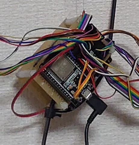
The prototype, with the wiring hanging out (before)
Problems:
- The wiring is a mess to look at
- Intermittent connections are easy to get
- It cannot be hung on a wall
- Not something you want to run long term
What a PCB buys you:
- ✅ Compact, and it looks finished
- ✅ Reliable connections
- ✅ Something you would actually put in a room
- ✅ You learn to design boards
So let’s build it properly.
Parts and Tools
Bill of materials
| Part | Qty | Approx. price (2026) | Notes |
|---|---|---|---|
| TZ-250A LCD display unit | 6 | from ¥3,000 (used) | Sold as surplus stock; see the note below |
| ESP32-WROOM-32 dev board | 1 | from ¥600 | Widely available from hobby distributors |
| RTC-8564NB RTC module | 1 | ¥280 | Epson Toyocom RTC |
| MCP23017 I2C I/O expander | 3 | ¥120 × 3 = ¥360 | 28-pin DIP |
| 28-pin DIP socket | 3 | ¥50 × 3 = ¥150 | For the MCP23017s |
| CR2032 coin cell | 1 | ¥100 | RTC backup |
| 24 V relay module | 1 | from ¥300 | For the lamp |
| Piezo buzzer | 1 | ¥100 | Alarm sound |
| Assorted resistors and capacitors | as needed | from ¥500 | — |
| PCB (ordered from JLCPCB) | 5 | from $7.90 | See the ordering section |
Rough total: around ¥5,000–7,000, depending on what the used LCDs cost.
(Prices are Japanese retail as of 2026, given for scale rather than as a shopping list.)
Software and tools
| Tool | Version | Purpose |
|---|---|---|
| Arduino IDE | 2.3 or later | Firmware development |
| KiCad | 8.0 or later | PCB design |
| Arduino libraries needed | - | Adafruit MCP23017, Wire, WiFi |
The star of the project: the large LCD panels
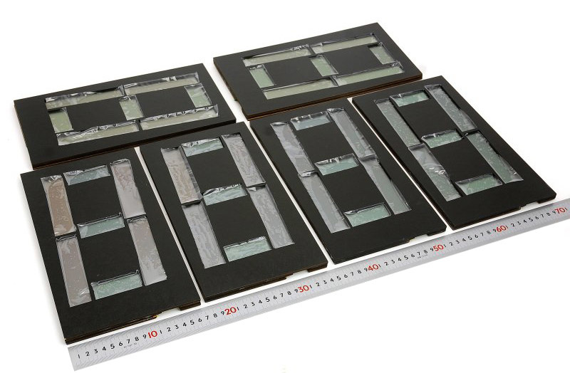
The TZ-250A seven-segment-style LCD panel — very legible
TZ-250A characteristics:
- Size: roughly 60 mm × 90 mm each
- Display: large seven-segment-style digits
- Control: 4-bit parallel data plus control signals
- Power: extremely low consumption
Six of these panels display HH:MM:SS.
On sourcing them: These turn up as surplus/used stock and availability is unpredictable — if you find some, grab them. If you cannot, a MAX7219-driven seven-segment LED module is a workable substitute, though the circuit needs changing to suit.
Understanding the System
Before laying out a board, it helps to have the whole system straight.
Block diagram
┌─────────────┐
│   Wi-Fi     │ ← time fetched from an NTP server
│   Router    │
└──────┬──────┘
       │ Wi-Fi
┌──────▼─────────┐
│  ESP32-WROOM   │ ← main microcontroller
│  - timekeeping │
│  - Wi-Fi       │
│  - I2C master  │
└────┬───┬───┬──┘
     │   │   │ I2C
 ┌───▼┐ ┌▼──┐ ┌▼──┐
 │MCP │ │MCP│ │MCP│ ← I/O expanders
 │#0  │ │#1 │ │#2 │   (GPIO expansion)
 └┬──┬┘ └┬─┬┘ └┬─┬┘
  │  │   │ │   │ │
┌▼┐┌▼┐ ┌▼┐▼┐ ┌▼┐▼┐
│L││L│ │L││L│ │L││L│ ← LCD × 6
│C││C│ │C││C│ │C││C│   (HH:MM:SS)
│D││D│ │D││D│ │D││D│
└─┘└─┘ └─┘─┘ └─┘─┘
Why an I/O expander is necessary
The problem: each LCD panel needs 7 pins → 6 panels × 7 pins = 42 GPIO pins
What the ESP32 offers: around 20 pins you can realistically use → nowhere near enough
The fix: MCP23017 I/O expanders
- 16 extra GPIOs for the cost of two I2C wires
- Three of them gives you 48 GPIOs
- Multiple devices coexist by changing the I2C address
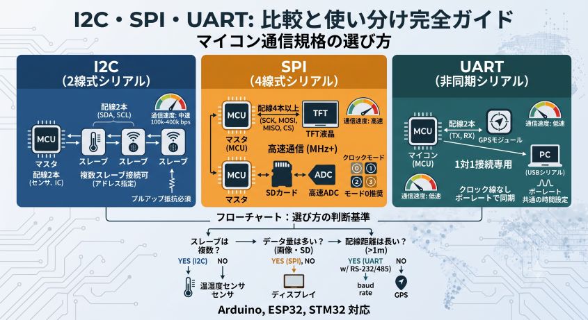
If the reasoning behind I2C addresses and pull-up resistors is not yet familiar, I2C vs SPI vs UART: Wiring, Speed, and How to Choose covers why the bus works this way. For the MCP23017 specifically — address selection and sample code — see MCP23017 with ESP32: I2C Address Setup and 16 GPIO Pins.
How timekeeping works
- At boot: connect to Wi-Fi → fetch the current time from an NTP server
- Set the RTC: write that time into the RTC-8564NB
- Normal operation: read the time back from the RTC and display it
- During a power cut: the RTC’s backup battery keeps time running
💡 The point: with an RTC fitted, the clock still works as a clock even where Wi-Fi is unavailable.
Building the Prototype Circuit
Before committing to a PCB, the whole thing was built on a breadboard.
The prototype as a whole
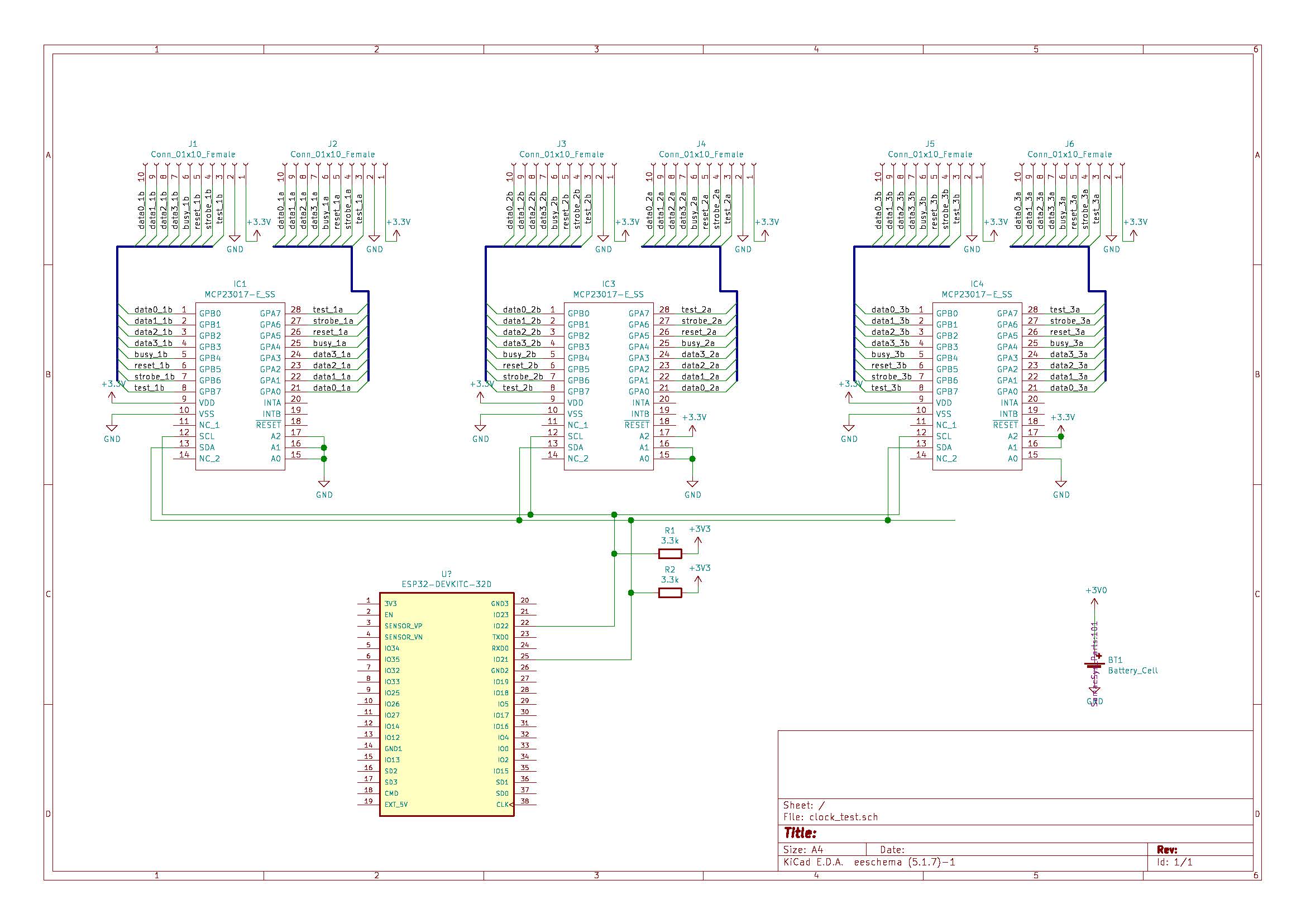
The breadboard prototype
The perfboard build (before the PCB)
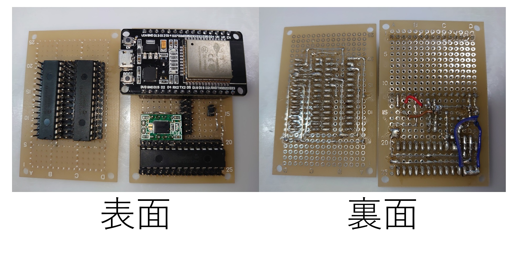
The prototype on perfboard
Plenty of jumper wire and not much to look at, but more than good enough to prove the design.
Key points of the circuit
1. ESP32 to MCP23017 (I2C)
| ESP32 pin | Connects to | Description |
|---|---|---|
| GPIO21 (SDA) | MCP23017 SDA | I2C data line |
| GPIO22 (SCL) | MCP23017 SCL | I2C clock |
| 3.3 V | MCP23017 VDD | Supply |
| GND | MCP23017 VSS | Ground |
2. Setting the MCP23017 addresses
The three MCP23017s are told apart by their I2C addresses.
| Device | A0 | A1 | A2 | I2C address |
|---|---|---|---|---|
| MCP #0 | GND | GND | GND | 0x20 |
| MCP #1 | VCC | GND | GND | 0x21 |
| MCP #2 | VCC | VCC | GND | 0x23 |
💡 How it is set: tie the A0, A1 and A2 pins of each MCP23017 to VCC or GND to fix its address.
3. MCP23017 to LCD
Each MCP23017 drives two LCD panels.
Connections per LCD panel:
| MCP23017 pin | LCD pin | Signal | Description |
|---|---|---|---|
| GPA0 | D0 | Data 0 | Data bit 0 |
| GPA1 | D1 | Data 1 | Data bit 1 |
| GPA2 | D2 | Data 2 | Data bit 2 |
| GPA3 | D3 | Data 3 | Data bit 3 |
| GPA4 | BSY | Busy | LCD busy flag (input) |
| GPA5 | RST | Reset | LCD initialization |
| GPA6 | STR | Strobe | Write trigger |
With 16 GPIOs per MCP23017, 8 pins × 2 panels = 16 pins drives two LCDs from one chip.
4. Connecting the RTC module
| RTC-8564NB | ESP32 | Description |
|---|---|---|
| SDA | GPIO21 | I2C data (shared with the MCP23017s) |
| SCL | GPIO22 | I2C clock (shared with the MCP23017s) |
| VDD | 3.3 V | Supply |
| VSS | GND | Ground |
Backup battery: fit a CR2032 and the clock keeps time while the main supply is off.
Writing the Arduino Program
What the program does
The firmware handles the following:
- Wi-Fi: connect using the configured SSID and password
- NTP: fetch the current time with
configTime() - RTC init: write the fetched time into the RTC
- MCP23017 init: configure the three I/O expanders
- LCD init: send the reset signal
- Main loop: read the time from the RTC and drive the LCDs
Libraries required
Install these from the Library Manager in Arduino IDE 2.x:
- Adafruit MCP23017 Arduino Library by Adafruit
- WiFi (bundled with the ESP32 core, no install needed)
- Wire (I2C, a standard library)
The program code
💡 Note: the full sketch runs to over 800 lines, so the walkthrough below picks out the parts that matter.
📄 Click to show the full sketch (collapsed — it is long)
#include <WiFi.h>
#include <Wire.h>
#include<time.h>
#include <stdlib.h>
#include <stdio.h>
#include "Adafruit_MCP23017.h"
Adafruit_MCP23017 mcp0;
Adafruit_MCP23017 mcp1;
Adafruit_MCP23017 mcp2;
char *ssid = "SSID";
char *pass = "PASSWORD";
int ihour, imin, isec, i;
int h1, h2, m1, m2, s1, s2;
char hour, minute, sec;
int RegTbl[16];
byte RTC8564 = 0x51;
struct tm timeInfo;//object that holds the time
char s[20];//string buffer

int s0_D0_Pin = 0; //data line 0, out
int s0_D1_Pin = 1; //data line 1, out
int s0_D2_Pin = 2; //data line 2, out
int s0_D3_Pin = 3; //data line 3, out
int s0_Bsy_Pin = 4; //BUSY signal, in
int s0_Rst_Pin = 5; //RESET signal, normally LOW, out
int s0_Str_Pin = 6; //STROBE signal, out

int s1_D0_Pin = 8; //data line 0, out
int s1_D1_Pin = 9; //data line 1, out
int s1_D2_Pin = 10; //data line 2, out
int s1_D3_Pin = 11; //data line 3, out
int s1_Bsy_Pin = 12; //BUSY signal, in
int s1_Rst_Pin = 13; //RESET signal, normally LOW, out
int s1_Str_Pin = 14; //STROBE signal, out

int s2_D0_Pin = 0; //data line 0, out
int s2_D1_Pin = 1; //data line 1, out
int s2_D2_Pin = 2; //data line 2, out
int s2_D3_Pin = 3; //data line 3, out
int s2_Bsy_Pin = 4; //BUSY signal, in
int s2_Rst_Pin = 5; //RESET signal, normally LOW, out
int s2_Str_Pin = 6; //STROBE signal, out

int s3_D0_Pin = 8; //data line 0, out
int s3_D1_Pin = 9; //data line 1, out
int s3_D2_Pin = 10; //data line 2, out
int s3_D3_Pin = 11; //data line 3, out
int s3_Bsy_Pin = 12; //BUSY signal, in
int s3_Rst_Pin = 13; //RESET signal, normally LOW, out
int s3_Str_Pin = 14; //STROBE signal, out

int s4_D0_Pin = 0; //data line 0, out
int s4_D1_Pin = 1; //data line 1, out
int s4_D2_Pin = 2; //data line 2, out
int s4_D3_Pin = 3; //data line 3, out
int s4_Bsy_Pin = 4; //BUSY signal, in
int s4_Rst_Pin = 5; //RESET signal, normally LOW, out
int s4_Str_Pin = 6; //STROBE signal, out

int s5_D0_Pin = 8; //data line 0, out
int s5_D1_Pin = 9; //data line 1, out
int s5_D2_Pin = 10; //data line 2, out
int s5_D3_Pin = 11; //data line 3, out
int s5_Bsy_Pin = 12; //BUSY signal, in
int s5_Rst_Pin = 13; //RESET signal, normally LOW, out
int s5_Str_Pin = 14; //STROBE signal, out

//display data definitions
int disp_0[8] = {0, 0, 0, 0, 0, 0, 0, 1};
int disp_1[8] = {1, 0, 0, 0, 0, 0, 0, 1};
int disp_2[8] = {0, 1, 0, 0, 0, 0, 0, 1};
int disp_3[8] = {1, 1, 0, 0, 0, 0, 0, 1};
int disp_4[8] = {0, 0, 1, 0, 0, 0, 0, 1};
int disp_5[8] = {1, 0, 1, 0, 0, 0, 0, 1};
int disp_6[8] = {0, 1, 1, 0, 0, 0, 0, 1};
int disp_7[8] = {1, 1, 1, 0, 0, 0, 0, 1};
int disp_8[8] = {0, 0, 0, 0, 1, 0, 0, 1};
int disp_9[8] = {1, 0, 0, 0, 1, 0, 0, 1};
int disp_A[8] = {0, 1, 0, 0, 1, 0, 0, 1};
int disp_B[8] = {1, 1, 0, 0, 1, 0, 0, 1};
int disp_C[8] = {0, 0, 1, 0, 1, 0, 0, 1};
int disp_D[8] = {1, 0, 1, 0, 1, 0, 0, 1};
int disp_E[8] = {0, 1, 1, 0, 1, 0, 0, 1};
int disp_F[8] = {1, 1, 1, 0, 1, 0, 0, 1};

int disp_H[8] = {1, 0, 0, 0, 0, 1, 0, 1};
int disp_I[8] = {0, 1, 0, 0, 0, 1, 0, 1};
int disp_J[8] = {1, 1, 0, 0, 0, 1, 0, 1};
int disp_L[8] = {1, 0, 1, 0, 0, 1, 0, 1};
int disp_O[8] = {0, 0, 0, 0, 1, 1, 0, 1};
int disp_P[8] = {1, 0, 0, 0, 1, 1, 0, 1};
int disp_S[8] = {0, 0, 1, 0, 1, 1, 0, 1};
int disp_U[8] = {0, 1, 1, 0, 1, 1, 0, 1};
int disp_BL[8] = {0, 0, 1, 0, 0, 0, 1, 1};
int disp_RR[8] = {0, 1, 1, 0, 0, 0, 1, 1};
int disp_RL[8] = {1, 1, 1, 0, 0, 0, 1, 1};


// DECIMAL -> BCD
byte dec2bcd( byte data )
{
  return ((( data / 10) << 4) + (data % 10));
}
// BCD -> DECIMAL
byte BCDtoDec(byte data) {
  return ((data >> 4) * 10) + (data & 0x0F) ;
}


void init_pin() {
  //set every pin LOW
  mcp0.digitalWrite(s0_D0_Pin, LOW);
  mcp0.digitalWrite(s0_D1_Pin, LOW);
  mcp0.digitalWrite(s0_D2_Pin, LOW);
  mcp0.digitalWrite(s0_D3_Pin, LOW);
  mcp0.digitalWrite(s0_Str_Pin, LOW);
  mcp0.digitalWrite(s0_Rst_Pin, LOW);
  mcp0.digitalWrite(s1_D0_Pin, LOW);
  mcp0.digitalWrite(s1_D1_Pin, LOW);
  mcp0.digitalWrite(s1_D2_Pin, LOW);
  mcp0.digitalWrite(s1_D3_Pin, LOW);
  mcp0.digitalWrite(s1_Str_Pin, LOW);
  mcp0.digitalWrite(s1_Rst_Pin, LOW);
  delay(100);
  mcp1.digitalWrite(s2_D0_Pin, LOW);
  mcp1.digitalWrite(s2_D1_Pin, LOW);
  mcp1.digitalWrite(s2_D2_Pin, LOW);
  mcp1.digitalWrite(s2_D3_Pin, LOW);
  mcp1.digitalWrite(s2_Str_Pin, LOW);
  mcp1.digitalWrite(s2_Rst_Pin, LOW);
  mcp1.digitalWrite(s3_D0_Pin, LOW);
  mcp1.digitalWrite(s3_D1_Pin, LOW);
  mcp1.digitalWrite(s3_D2_Pin, LOW);
  mcp1.digitalWrite(s3_D3_Pin, LOW);
  mcp1.digitalWrite(s3_Str_Pin, LOW);
  mcp1.digitalWrite(s3_Rst_Pin, LOW);
  delay(100);
  mcp2.digitalWrite(s4_D0_Pin, LOW);
  mcp2.digitalWrite(s4_D1_Pin, LOW);
  mcp2.digitalWrite(s4_D2_Pin, LOW);
  mcp2.digitalWrite(s4_D3_Pin, LOW);
  mcp2.digitalWrite(s4_Str_Pin, LOW);
  mcp2.digitalWrite(s4_Rst_Pin, LOW);
  mcp2.digitalWrite(s5_D0_Pin, LOW);
  mcp2.digitalWrite(s5_D1_Pin, LOW);
  mcp2.digitalWrite(s5_D2_Pin, LOW);
  mcp2.digitalWrite(s5_D3_Pin, LOW);
  mcp2.digitalWrite(s5_Str_Pin, LOW);
  mcp2.digitalWrite(s5_Rst_Pin, LOW);
  delay(100);
  //assert reset
  mcp0.digitalWrite(s0_Rst_Pin, HIGH);
  mcp0.digitalWrite(s1_Rst_Pin, HIGH);
  delay(100);
  mcp1.digitalWrite(s2_Rst_Pin, HIGH);
  mcp1.digitalWrite(s3_Rst_Pin, HIGH);
  delay(100);
  mcp2.digitalWrite(s4_Rst_Pin, HIGH);
  mcp2.digitalWrite(s5_Rst_Pin, HIGH);
  delay(1000);
  mcp0.digitalWrite(s0_Rst_Pin, LOW);
  mcp0.digitalWrite(s1_Rst_Pin, LOW);
  delay(100);
  mcp1.digitalWrite(s2_Rst_Pin, LOW);
  mcp1.digitalWrite(s3_Rst_Pin, LOW);
  delay(100);
  mcp2.digitalWrite(s4_Rst_Pin, LOW);
  mcp2.digitalWrite(s5_Rst_Pin, LOW);
  delay(1000);
}


void write_display0(int disp_data) {
  int i;
  int val = 0;
  int data[8];

  switch (disp_data) {
    case 0:    memcpy(data, disp_0, sizeof(int) * 8);    break;
    case 1:    memcpy(data, disp_1, sizeof(int) * 8);    break;
    case 2:    memcpy(data, disp_2, sizeof(int) * 8);    break;
    case 3:    memcpy(data, disp_3, sizeof(int) * 8);    break;
    case 4:    memcpy(data, disp_4, sizeof(int) * 8);    break;
    case 5:    memcpy(data, disp_5, sizeof(int) * 8);    break;
    case 6:    memcpy(data, disp_6, sizeof(int) * 8);    break;
    case 7:    memcpy(data, disp_7, sizeof(int) * 8);    break;
    case 8:    memcpy(data, disp_8, sizeof(int) * 8);    break;
    case 9:    memcpy(data, disp_9, sizeof(int) * 8);    break;
  }

  while (mcp0.digitalRead(s0_Bsy_Pin) != LOW)
    continue;
  //write the LOW nibble
  mcp0.digitalWrite(s0_D0_Pin, data[0]);
  mcp0.digitalWrite(s0_D1_Pin, data[1]);
  mcp0.digitalWrite(s0_D2_Pin, data[2]);
  mcp0.digitalWrite(s0_D3_Pin, data[3]);
  mcp0.digitalWrite(s0_Str_Pin, HIGH);
  while (mcp0.digitalRead(s0_Bsy_Pin) != HIGH)
    continue;
  mcp0.digitalWrite(s0_Str_Pin, LOW);
  while (mcp0.digitalRead(s0_Bsy_Pin) != LOW)
    continue;
  mcp0.digitalWrite(s0_D0_Pin, data[4]);
  mcp0.digitalWrite(s0_D1_Pin, data[5]);
  mcp0.digitalWrite(s0_D2_Pin, data[6]);
  mcp0.digitalWrite(s0_D3_Pin, data[7]);
  delay(10);
  mcp0.digitalWrite(s0_Str_Pin, HIGH);
  while (mcp0.digitalRead(s0_Bsy_Pin) != HIGH)
    continue;
  mcp0.digitalWrite(s0_Str_Pin, LOW);

}

void write_display1(int disp_data) {
  int i;
  int val = 0;
  int data[8];

  switch (disp_data) {
    case 0:    memcpy(data, disp_0, sizeof(int) * 8);    break;
    case 1:    memcpy(data, disp_1, sizeof(int) * 8);    break;
    case 2:    memcpy(data, disp_2, sizeof(int) * 8);    break;
    case 3:    memcpy(data, disp_3, sizeof(int) * 8);    break;
    case 4:    memcpy(data, disp_4, sizeof(int) * 8);    break;
    case 5:    memcpy(data, disp_5, sizeof(int) * 8);    break;
    case 6:    memcpy(data, disp_6, sizeof(int) * 8);    break;
    case 7:    memcpy(data, disp_7, sizeof(int) * 8);    break;
    case 8:    memcpy(data, disp_8, sizeof(int) * 8);    break;
    case 9:    memcpy(data, disp_9, sizeof(int) * 8);    break;
  }

  while (mcp0.digitalRead(s1_Bsy_Pin) != LOW)
    continue;
  mcp0.digitalWrite(s1_D0_Pin, data[0]);
  mcp0.digitalWrite(s1_D1_Pin, data[1]);
  mcp0.digitalWrite(s1_D2_Pin, data[2]);
  mcp0.digitalWrite(s1_D3_Pin, data[3]);
  mcp0.digitalWrite(s1_Str_Pin, HIGH);
  while (mcp0.digitalRead(s1_Bsy_Pin) != HIGH)
    continue;
  mcp0.digitalWrite(s1_Str_Pin, LOW);
  while (mcp0.digitalRead(s1_Bsy_Pin) != LOW)
    continue;
  mcp0.digitalWrite(s1_D0_Pin, data[4]);
  mcp0.digitalWrite(s1_D1_Pin, data[5]);
  mcp0.digitalWrite(s1_D2_Pin, data[6]);
  mcp0.digitalWrite(s1_D3_Pin, data[7]);
  delay(10);

  mcp0.digitalWrite(s1_Str_Pin, HIGH);
  while (mcp0.digitalRead(s1_Bsy_Pin) != HIGH)
    continue;
  mcp0.digitalWrite(s1_Str_Pin, LOW);

}


void write_display2(int disp_data) {
  int i;
  int val = 0;
  int data[8];

  switch (disp_data) {
    case 0:    memcpy(data, disp_0, sizeof(int) * 8);    break;
    case 1:    memcpy(data, disp_1, sizeof(int) * 8);    break;
    case 2:    memcpy(data, disp_2, sizeof(int) * 8);    break;
    case 3:    memcpy(data, disp_3, sizeof(int) * 8);    break;
    case 4:    memcpy(data, disp_4, sizeof(int) * 8);    break;
    case 5:    memcpy(data, disp_5, sizeof(int) * 8);    break;
    case 6:    memcpy(data, disp_6, sizeof(int) * 8);    break;
    case 7:    memcpy(data, disp_7, sizeof(int) * 8);    break;
    case 8:    memcpy(data, disp_8, sizeof(int) * 8);    break;
    case 9:    memcpy(data, disp_9, sizeof(int) * 8);    break;
  }
  while (mcp1.digitalRead(s2_Bsy_Pin) != LOW)
    continue;
  //write the LOW nibble

  mcp1.digitalWrite(s2_D0_Pin, data[0]);
  mcp1.digitalWrite(s2_D1_Pin, data[1]);
  mcp1.digitalWrite(s2_D2_Pin, data[2]);
  mcp1.digitalWrite(s2_D3_Pin, data[3]);
  mcp1.digitalWrite(s2_Str_Pin, HIGH);
  while (mcp1.digitalRead(s2_Bsy_Pin) != HIGH)
    continue;
  mcp1.digitalWrite(s2_Str_Pin, LOW);
  while (mcp1.digitalRead(s2_Bsy_Pin) != LOW)
    continue;
  mcp1.digitalWrite(s2_D0_Pin, data[4]);
  mcp1.digitalWrite(s2_D1_Pin, data[5]);
  mcp1.digitalWrite(s2_D2_Pin, data[6]);
  mcp1.digitalWrite(s2_D3_Pin, data[7]);
  delay(10);
  mcp1.digitalWrite(s2_Str_Pin, HIGH);
  while (mcp1.digitalRead(s2_Bsy_Pin) != HIGH)
    continue;
  mcp1.digitalWrite(s2_Str_Pin, LOW);

}

void write_display3(int disp_data) {
  int i;
  int val = 0;
  int data[8];

  switch (disp_data) {
    case 0:    memcpy(data, disp_0, sizeof(int) * 8);    break;
    case 1:    memcpy(data, disp_1, sizeof(int) * 8);    break;
    case 2:    memcpy(data, disp_2, sizeof(int) * 8);    break;
    case 3:    memcpy(data, disp_3, sizeof(int) * 8);    break;
    case 4:    memcpy(data, disp_4, sizeof(int) * 8);    break;
    case 5:    memcpy(data, disp_5, sizeof(int) * 8);    break;
    case 6:    memcpy(data, disp_6, sizeof(int) * 8);    break;
    case 7:    memcpy(data, disp_7, sizeof(int) * 8);    break;
    case 8:    memcpy(data, disp_8, sizeof(int) * 8);    break;
    case 9:    memcpy(data, disp_9, sizeof(int) * 8);    break;
  }

  while (mcp1.digitalRead(s3_Bsy_Pin) != LOW)
    continue;
  mcp1.digitalWrite(s3_D0_Pin, data[0]);
  mcp1.digitalWrite(s3_D1_Pin, data[1]);
  mcp1.digitalWrite(s3_D2_Pin, data[2]);
  mcp1.digitalWrite(s3_D3_Pin, data[3]);
  mcp1.digitalWrite(s3_Str_Pin, HIGH);

  while (mcp1.digitalRead(s3_Bsy_Pin) != HIGH)
    continue;
  mcp1.digitalWrite(s3_Str_Pin, LOW);
  while (mcp1.digitalRead(s3_Bsy_Pin) != LOW)
    continue;
  mcp1.digitalWrite(s3_D0_Pin, data[4]);
  mcp1.digitalWrite(s3_D1_Pin, data[5]);
  mcp1.digitalWrite(s3_D2_Pin, data[6]);
  mcp1.digitalWrite(s3_D3_Pin, data[7]);
  delay(10);

  mcp1.digitalWrite(s3_Str_Pin, HIGH);
  while (mcp1.digitalRead(s3_Bsy_Pin) != HIGH)
    continue;
  mcp1.digitalWrite(s3_Str_Pin, LOW);

}


void write_display4(int disp_data) {
  int i;
  int val = 0;
  int data[8];

  switch (disp_data) {
    case 0:    memcpy(data, disp_0, sizeof(int) * 8);    break;
    case 1:    memcpy(data, disp_1, sizeof(int) * 8);    break;
    case 2:    memcpy(data, disp_2, sizeof(int) * 8);    break;
    case 3:    memcpy(data, disp_3, sizeof(int) * 8);    break;
    case 4:    memcpy(data, disp_4, sizeof(int) * 8);    break;
    case 5:    memcpy(data, disp_5, sizeof(int) * 8);    break;
    case 6:    memcpy(data, disp_6, sizeof(int) * 8);    break;
    case 7:    memcpy(data, disp_7, sizeof(int) * 8);    break;
    case 8:    memcpy(data, disp_8, sizeof(int) * 8);    break;
    case 9:    memcpy(data, disp_9, sizeof(int) * 8);    break;
  }

  while (mcp2.digitalRead(s4_Bsy_Pin) != LOW)
    continue;
  //write the LOW nibble
  mcp2.digitalWrite(s4_D0_Pin, data[0]);
  mcp2.digitalWrite(s4_D1_Pin, data[1]);
  mcp2.digitalWrite(s4_D2_Pin, data[2]);
  mcp2.digitalWrite(s4_D3_Pin, data[3]);
  mcp2.digitalWrite(s4_Str_Pin, HIGH);
  while (mcp2.digitalRead(s4_Bsy_Pin) != HIGH)
    continue;
  mcp2.digitalWrite(s4_Str_Pin, LOW);
  while (mcp2.digitalRead(s4_Bsy_Pin) != LOW)
    continue;
  mcp2.digitalWrite(s4_D0_Pin, data[4]);
  mcp2.digitalWrite(s4_D1_Pin, data[5]);
  mcp2.digitalWrite(s4_D2_Pin, data[6]);
  mcp2.digitalWrite(s4_D3_Pin, data[7]);
  delay(10);
  mcp2.digitalWrite(s4_Str_Pin, HIGH);
  while (mcp2.digitalRead(s4_Bsy_Pin) != HIGH)
    continue;
  mcp2.digitalWrite(s4_Str_Pin, LOW);

}

void write_display5(int disp_data) {
  int i;
  int val = 0;
  int data[8];

  switch (disp_data) {
    case 0:    memcpy(data, disp_0, sizeof(int) * 8);    break;
    case 1:    memcpy(data, disp_1, sizeof(int) * 8);    break;
    case 2:    memcpy(data, disp_2, sizeof(int) * 8);    break;
    case 3:    memcpy(data, disp_3, sizeof(int) * 8);    break;
    case 4:    memcpy(data, disp_4, sizeof(int) * 8);    break;
    case 5:    memcpy(data, disp_5, sizeof(int) * 8);    break;
    case 6:    memcpy(data, disp_6, sizeof(int) * 8);    break;
    case 7:    memcpy(data, disp_7, sizeof(int) * 8);    break;
    case 8:    memcpy(data, disp_8, sizeof(int) * 8);    break;
    case 9:    memcpy(data, disp_9, sizeof(int) * 8);    break;
  }

  while (mcp2.digitalRead(s5_Bsy_Pin) != LOW)
    continue;
  mcp2.digitalWrite(s5_D0_Pin, data[0]);
  mcp2.digitalWrite(s5_D1_Pin, data[1]);
  mcp2.digitalWrite(s5_D2_Pin, data[2]);
  mcp2.digitalWrite(s5_D3_Pin, data[3]);
  mcp2.digitalWrite(s5_Str_Pin, HIGH);
  while (mcp2.digitalRead(s5_Bsy_Pin) != HIGH)
    continue;
  mcp2.digitalWrite(s5_Str_Pin, LOW);
  while (mcp2.digitalRead(s5_Bsy_Pin) != LOW)
    continue;
  mcp2.digitalWrite(s5_D0_Pin, data[4]);
  mcp2.digitalWrite(s5_D1_Pin, data[5]);
  mcp2.digitalWrite(s5_D2_Pin, data[6]);
  mcp2.digitalWrite(s5_D3_Pin, data[7]);
  delay(10);

  mcp2.digitalWrite(s5_Str_Pin, HIGH);
  while (mcp2.digitalRead(s5_Bsy_Pin) != HIGH)
    continue;
  mcp2.digitalWrite(s5_Str_Pin, LOW);

}

void setup() {
  // initialize the digital pin as an output.
  Serial.begin(115200);
  Wire.begin();

  WiFi.mode(WIFI_STA);
  WiFi.disconnect();
  if (WiFi.begin(ssid, pass) != WL_DISCONNECTED) {
    ESP.restart();
  }
  while (WiFi.status() != WL_CONNECTED) {
    delay(1000);
  }

  Serial.println("Connected to the WiFi network!");
  delay(1000);
  configTime(9 * 3600L, 0, "ntp.nict.jp", "time.google.com", "ntp.jst.mfeed.ad.jp");//NTP configuration
  getLocalTime(&timeInfo);//load the current time into the tm object timeInfo


  delay(1);
  ihour = timeInfo.tm_hour;
  imin = timeInfo.tm_min;
  isec = timeInfo.tm_sec;
  sprintf(s, " %04d/%02d/%02d %02d:%02d:%02d",
          timeInfo.tm_year + 1900, timeInfo.tm_mon + 1, timeInfo.tm_mday,
          timeInfo.tm_hour, timeInfo.tm_min, timeInfo.tm_sec);//convert to a human-readable format
  Serial.println(s);//print the time to the serial monitor


  Wire.beginTransmission(RTC8564);
  Wire.write(0x00);
  Wire.write(0x00);// [00]Control1
  Wire.write(0x02);// [01]Control2
  Wire.write(byte(dec2bcd(isec)));// [02]Seconds(15 s)
  Wire.write(byte(dec2bcd(imin))); // [03]Minutes(20 min)
  Wire.write(byte(dec2bcd(ihour)));// [04]Hours(12 h)
  Wire.write(0x25);// [05]Days(25th)
  Wire.write(0x01);    // [06]Weekdays(Monday)
  Wire.write(0x12 | 0x80); // [07]Month/Century(December, 21st century)
  Wire.write(0x17);// [08]Years(2017)
  Wire.endTransmission();
  delay(10);

  Wire.beginTransmission(RTC8564);
  Wire.write(0x00);
  Wire.endTransmission();
  Wire.requestFrom(RTC8564, 16);
  for (i = 0; i < 16; i++) {
    while (Wire.available() == 0 ) {}
    RegTbl[i] = Wire.read();
  }
  ihour = (BCDtoDec(RegTbl[4] & 0x3F));
  imin = (BCDtoDec(RegTbl[3] & 0x7F));
  isec = (BCDtoDec(RegTbl[2] & 0x7F));


  mcp0.begin();
  mcp1.begin(0x01);
  mcp2.begin(0x03);

  mcp0.pinMode(s0_D0_Pin, OUTPUT);
  mcp0.pinMode(s0_D1_Pin, OUTPUT);
  mcp0.pinMode(s0_D2_Pin, OUTPUT);
  mcp0.pinMode(s0_D3_Pin, OUTPUT);
  mcp0.pinMode(s0_Bsy_Pin, INPUT);
  mcp0.pinMode(s0_Str_Pin, OUTPUT);
  mcp0.pinMode(s0_Rst_Pin, OUTPUT);

  mcp0.pinMode(s1_D0_Pin, OUTPUT);
  mcp0.pinMode(s1_D1_Pin, OUTPUT);
  mcp0.pinMode(s1_D2_Pin, OUTPUT);
  mcp0.pinMode(s1_D3_Pin, OUTPUT);
  mcp0.pinMode(s1_Bsy_Pin, INPUT);
  mcp0.pinMode(s1_Str_Pin, OUTPUT);
  mcp0.pinMode(s1_Rst_Pin, OUTPUT);

  mcp1.pinMode(s2_D0_Pin, OUTPUT);
  mcp1.pinMode(s2_D1_Pin, OUTPUT);
  mcp1.pinMode(s2_D2_Pin, OUTPUT);
  mcp1.pinMode(s2_D3_Pin, OUTPUT);
  mcp1.pinMode(s2_Bsy_Pin, INPUT);
  mcp1.pinMode(s2_Str_Pin, OUTPUT);
  mcp1.pinMode(s2_Rst_Pin, OUTPUT);

  mcp1.pinMode(s3_D0_Pin, OUTPUT);
  mcp1.pinMode(s3_D1_Pin, OUTPUT);
  mcp1.pinMode(s3_D2_Pin, OUTPUT);
  mcp1.pinMode(s3_D3_Pin, OUTPUT);
  mcp1.pinMode(s3_Bsy_Pin, INPUT);
  mcp1.pinMode(s3_Str_Pin, OUTPUT);
  mcp1.pinMode(s3_Rst_Pin, OUTPUT);

  mcp2.pinMode(s4_D0_Pin, OUTPUT);
  mcp2.pinMode(s4_D1_Pin, OUTPUT);
  mcp2.pinMode(s4_D2_Pin, OUTPUT);
  mcp2.pinMode(s4_D3_Pin, OUTPUT);
  mcp2.pinMode(s4_Bsy_Pin, INPUT);
  mcp2.pinMode(s4_Str_Pin, OUTPUT);
  mcp2.pinMode(s4_Rst_Pin, OUTPUT);

  mcp2.pinMode(s5_D0_Pin, OUTPUT);
  mcp2.pinMode(s5_D1_Pin, OUTPUT);
  mcp2.pinMode(s5_D2_Pin, OUTPUT);
  mcp2.pinMode(s5_D3_Pin, OUTPUT);
  mcp2.pinMode(s5_Bsy_Pin, INPUT);
  mcp2.pinMode(s5_Str_Pin, OUTPUT);
  mcp2.pinMode(s5_Rst_Pin, OUTPUT);

  init_pin();
}

void loop() {
  Serial.println("LOOP");
  Wire.beginTransmission(RTC8564);
  Wire.write(0x00);
  Wire.endTransmission();
  Wire.requestFrom(RTC8564, 16);
  for (i = 0; i < 16; i++) {
    while (Wire.available() == 0 ) {}
    RegTbl[i] = Wire.read();
  }

  ihour = (BCDtoDec(RegTbl[4] & 0x3F));
  imin = (BCDtoDec(RegTbl[3] & 0x7F));
  isec = (BCDtoDec(RegTbl[2] & 0x7F));
  h1 = ihour / 10;
  h2 = ihour % 10;
  m1 = imin / 10;
  m2 = imin % 10;
  s1 = isec / 10;
  s2 = isec % 10;

  write_display0(h2);
  write_display1(h1);
  write_display2(s2);
  write_display3(s1);
  write_display4(m2);
  write_display5(m1);

  delay(100);
}
1. Wi-Fi connection and NTP time retrieval
// connect to Wi-Fi
WiFi.begin(ssid, pass);
while (WiFi.status() != WL_CONNECTED) {
  delay(1000);
}

// fetch the time over NTP (Japan Standard Time, GMT+9)
configTime(9 * 3600L, 0, "ntp.nict.jp", "time.google.com", "ntp.jst.mfeed.ad.jp");
getLocalTime(&timeInfo);
The NTP servers used:
ntp.nict.jp: Japan’s official NTP service (National Institute of Information and Communications Technology)time.google.com: Google’s public NTP servicentp.jst.mfeed.ad.jp: Internet Multifeed, in Japan
The code above is written for Japan: the first argument to configTime() is the UTC offset in seconds, so 9 * 3600L is UTC+9, and two of the three servers are Japanese. Change the offset to your own and swap in a nearby pool — pool.ntp.org works anywhere. Nothing else in the sketch depends on the region.
💡 The point: listing several NTP servers means one being unreachable does not stop you getting the time.
2. Writing the time into the RTC
// decimal → BCD
byte dec2bcd(byte data) {
  return (((data / 10) << 4) + (data % 10));
}

// write the time to the RTC
Wire.beginTransmission(RTC8564);
Wire.write(0x00);
Wire.write(0x00);                      // Control1
Wire.write(0x02);                      // Control2
Wire.write(byte(dec2bcd(isec)));       // seconds
Wire.write(byte(dec2bcd(imin)));       // minutes
Wire.write(byte(dec2bcd(ihour)));      // hours
Wire.endTransmission();
BCD (Binary-Coded Decimal): the RTC stores time in BCD. 23 o’clock, for instance, is stored as 0x23.
3. Initializing the MCP23017s
// initialize the three MCP23017s (addresses 0x20, 0x21, 0x23)
mcp0.begin();       // default address 0x20
mcp1.begin(0x01);   // address 0x21
mcp2.begin(0x03);   // address 0x23

// configure the GPIO directions
mcp0.pinMode(s0_D0_Pin, OUTPUT);   // data pin (output)
mcp0.pinMode(s0_Bsy_Pin, INPUT);   // busy signal (input)
// ... and so on for the remaining pins
4. The LCD display function
void write_display0(int disp_data) {
  // pick the data array matching the digit to be shown
  switch (disp_data) {
    case 0: memcpy(data, disp_0, sizeof(int) * 8); break;
    case 1: memcpy(data, disp_1, sizeof(int) * 8); break;
    // ... 0 through 9
  }

  // wait while the LCD is busy
  while (mcp0.digitalRead(s0_Bsy_Pin) != LOW) continue;

  // send the low nibble
  mcp0.digitalWrite(s0_D0_Pin, data[0]);
  mcp0.digitalWrite(s0_D1_Pin, data[1]);
  mcp0.digitalWrite(s0_D2_Pin, data[2]);
  mcp0.digitalWrite(s0_D3_Pin, data[3]);
  mcp0.digitalWrite(s0_Str_Pin, HIGH);  // strobe

  // wait for busy → send the high nibble
  // ... same again
}
💡 LCD timing: waiting for the BSY signal to go LOW is how the code confirms the LCD has finished the previous operation.
5. The main loop
void loop() {
  // read the time out of the RTC
  Wire.beginTransmission(RTC8564);
  Wire.write(0x00);
  Wire.endTransmission();
  Wire.requestFrom(RTC8564, 16);

  // BCD → decimal
  ihour = BCDtoDec(RegTbl[4] & 0x3F);
  imin = BCDtoDec(RegTbl[3] & 0x7F);
  isec = BCDtoDec(RegTbl[2] & 0x7F);

  // split into individual digits
  h1 = ihour / 10;  // tens of hours
  h2 = ihour % 10;  // units of hours
  m1 = imin / 10;   // tens of minutes
  m2 = imin % 10;   // units of minutes
  s1 = isec / 10;   // tens of seconds
  s2 = isec % 10;   // units of seconds

  // drive the six LCDs (left to right: HH:MM:SS)
  write_display5(h1);
  write_display4(h2);
  write_display3(m1);
  write_display2(m2);
  write_display1(s1);
  write_display0(s2);

  delay(100);  // 100 ms
}
Testing it
Flash the sketch and check that it runs.
Steps:
- Open the code in Arduino IDE 2.x
- Change the Wi-Fi SSID and password to match your network
- Select the ESP32 board (Tools → Board → ESP32 Dev Module)
- Select the port (Tools → Port)
- Upload (the “→” button, top left)
- Watch the Serial Monitor at 115200 baud
Example Serial Monitor output:
Connected to the WiFi network!
 2026/02/18 14:23:45
LOOP
LOOP
...
The prototype running
The time displays correctly. Functionally, it is finished.
But it does not look like much
Wiring everywhere — not a good look
Problems:
- The wiring is complicated and ugly
- The board dangles rather than mounts
- Doubtful it would survive long-term use
- It cannot go on a wall
The fix: turn it into a PCB and get something that looks and behaves like a product.
Designing the PCB in KiCad 8.x
Now for the board itself. As of 2026, KiCad 8.x is the current release and is considerably nicer to use than earlier versions.
Installing KiCad 8.x
- Go to the KiCad website
- Download the latest build for your OS (Windows / Mac / Linux)
- Run the installer
What’s new in KiCad 8.x (as of 2026):
- ✅ An improved user interface
- ✅ A faster 3D viewer
- ✅ A stronger Python API
- ✅ A larger component library
- ✅ Git integration
💡 For beginners: KiCad is a free, open-source, fully capable PCB design tool — and it is licensed for commercial work too.
The PCB design workflow
The process runs like this:
- Draw the schematic (Schematic Editor)
- Assign footprints (symbol to footprint assignment)
- Lay out the board (PCB Editor)
- Route the traces
- Run the design rule check (DRC)
- Export Gerber data
Step 1: the schematic
The first job is to redraw the prototype circuit in KiCad’s schematic editor.
Adding features the prototype did not have
The PCB gains an alarm function that the prototype never had.
Additional parts:
- Piezo buzzer: for the alarm sound
- 24 V relay: to switch the lamp
- Transistor (2SC1815 or similar): to drive the relay
- Diode (1N4148): flyback protection for the relay
The finished schematic
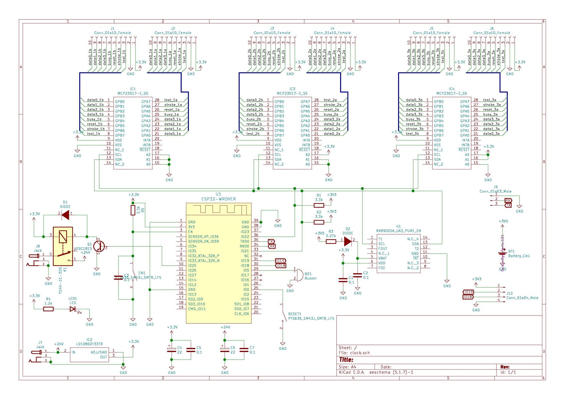
The schematic, drawn in KiCad 8.x
How the schematic breaks down:
| Block | Description |
|---|---|
| Power | 5 V in (USB or AC adapter) → 3.3 V conversion |
| MCU | ESP32-WROOM-32 plus supporting circuitry |
| I2C | MCP23017 × 3 + RTC-8564NB |
| LCD interface | MCP23017 → 6 LCD panels |
| Alarm | Buzzer + relay circuit |
💡 Schematic tips:
- Hierarchical sheets: break a complex circuit into sheets rather than one crowded page
- Net labels: fewer drawn wires, a much cleaner sheet
- Power symbols: use the dedicated VCC and GND symbols
Drawing the schematic in KiCad 8.x
- Start KiCad → New Project → name it
- Open the Schematic Editor
- Add Symbol (A): place the parts
- ESP32-WROOM-32
- MCP23017
- RTC-8564NB
- Connectors (for the LCD panels)
- Resistors, capacitors and so on
- Wire (W): connect the parts
- Net Label (L): label the nets (I2C_SDA, I2C_SCL, …)
- Electrical Rules Check (ERC): check the schematic for errors
Troubleshooting:
- Can’t find a part: pull it from KiCad’s official libraries, or from SnapEDA or Ultra Librarian
- ESP32 footprint: search the official library or GitHub for “ESP32-WROOM-32”
Step 2: assigning footprints
Every schematic symbol needs a physical footprint on the board.
Footprints for the main parts:
| Part | Footprint |
|---|---|
| ESP32-WROOM-32 | ESP32-WROOM-32 (38-pin SMD) |
| MCP23017 | DIP-28 (through-hole) |
| RTC-8564NB | DIP-8 or SMD |
| Resistors and capacitors | 1206 (SMD) or standard through-hole |
| Connectors | 2.54 mm pitch pin header |
💡 Worth knowing: through-hole parts (leads through holes) are far easier to work with if you are new to soldering. That is why the MCP23017s here are through-hole.
Step 3: board layout (component placement)
The PCB Editor is where parts get placed on the actual board.
Choosing the board size
The board here is 200 mm × 150 mm, driven by how the LCD panels have to sit.
💡 Cost tip: manufacturers like JLCPCB have their cheapest price bracket at 100 mm × 100 mm or smaller. Larger boards cost disproportionately more, so it is worth knowing where the boundary is.
Placement tips
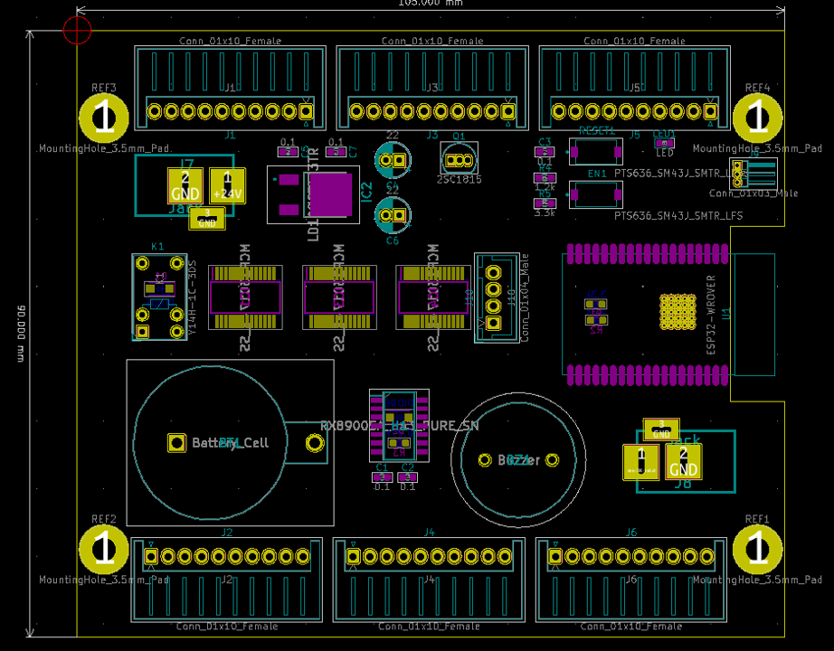
Component placement in KiCad 8.x
Placement principles:
- Group by function: ESP32 area, MCP23017 group, power section
- Think about height: put the LCD connectors along the board edge
- Place for routing: keep the I2C runs short
- Think about heat: leave clear space around the ESP32
- Mounting holes: 3 mm holes at the four corners (for M3 screws)
Handy KiCad 8.x features:
- 3D viewer: real-time 3D rendering (the 3D icon, top right)
- Push and shove: routing automatically nudges existing traces out of the way
- Design rules: trace width and clearance checked as you go
3D preview of the board
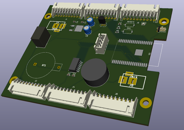
Top side (component side)
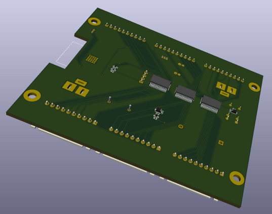
Bottom side (routing side)
You can see the finished thing before it exists. Checking in 3D catches part collisions and assembly mistakes before you spend money on the board.
Step 4: routing
With the parts placed, it is time to draw the traces.
Basic routing rules
| Item | Value | Notes |
|---|---|---|
| Power trace width | 0.5–1.0 mm | Carries larger current |
| Signal trace width | 0.25–0.4 mm | General signals |
| I2C trace width | 0.3 mm | For clean high-speed edges |
| Minimum clearance | 0.2 mm | JLCPCB’s manufacturing capability |
| Via diameter | 0.8 mm | Through-hole connection |
Routing tips:
- Power and ground first: route the fat traces before anything else
- Keep signals short: especially I2C, SPI and anything fast
- No right angles: route at 45° or with curves
- Do not force everything onto one layer: use both sides of a 2-layer board
Autorouting in KiCad 8.x:
- Route → Auto-route: fine for a simple circuit
- This board was routed by hand: complex boards come out better manually
Creating the ground plane
A ground plane (copper pour) fills the unused area with GND, which helps with noise and gives every return current a short path home.
How to add one (KiCad 8.x):
- Add Filled Zone (Ctrl+Shift+Z)
- Layer: B.Cu (bottom copper)
- Net: GND
- Clearance: 0.2 mm
- Draw the zone around the board outline
Step 5: design rule check (DRC)
Once routing is done, run the DRC (Design Rule Check) to find problems.
Running DRC:
- Inspect → Design Rules Checker
- Click Run DRC
- Fix whatever it finds
Common errors:
- Clearance violations: anything under 0.2 mm
- Pad collisions: parts placed too close together
- Unconnected nets: a trace you forgot
- Unfilled copper: a misconfigured ground plane
💡 Important: get DRC to zero errors before you order.
Generating the Gerber Data
With DRC clean, the next step is to produce the Gerber data the manufacturer needs.
What are Gerbers?
Gerber files are the PCB industry’s standard format, describing each layer of the board — copper, silkscreen, solder mask and so on — in a separate file.
Exporting Gerbers from KiCad 8.x
Step 1: plot settings
- In the PCB Editor, choose File → Plot
- The Plot dialog opens
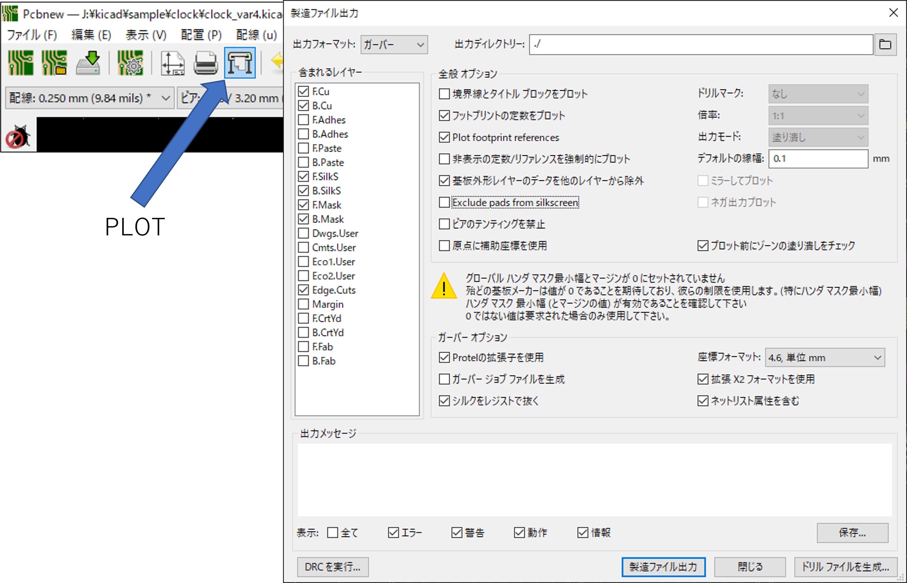
The plot dialog in KiCad 8.x
Step 2: choosing the layers
Tick the following:
| Layer | Description | Required |
|---|---|---|
| F.Cu | Front copper | ✅ |
| B.Cu | Back copper | ✅ |
| F.SilkS | Front silkscreen (part designators etc.) | ✅ |
| B.SilkS | Back silkscreen | △ |
| F.Mask | Front solder mask (the green area) | ✅ |
| B.Mask | Back solder mask | ✅ |
| Edge.Cuts | Board outline | ✅ |
| F.Paste | Front paste (for SMD stencils) | △ |
| B.Paste | Back paste | △ |
💡 Note: this is a 2-layer board, so F.Cu and B.Cu are the only copper layers. A 4-layer board adds In1.Cu and In2.Cu.
Step 3: output settings
| Setting | Recommended | Description |
|---|---|---|
| Plot format | Gerber | Gerber output |
| Output directory | gerber/ | Where the files go |
| Use Protel filename extensions | ☑ | Conventional extensions |
| Subtract soldermask from silkscreen | ☑ | Keeps silkscreen off the pads |
| Coordinate format | 4.6, unit mm | Coordinate precision |
Step 4: generating the files
- Click Plot
- Check the output messages
A successful run reports something like this:

Gerber generation complete
Files produced (example):
ESP32_Clock-F_Cu.gbr          # front copper
ESP32_Clock-B_Cu.gbr          # back copper
ESP32_Clock-F_SilkS.gbr       # front silkscreen
ESP32_Clock-B_SilkS.gbr       # back silkscreen
ESP32_Clock-F_Mask.gbr        # front solder mask
ESP32_Clock-B_Mask.gbr        # back solder mask
ESP32_Clock-Edge_Cuts.gbr     # board outline
Generating the drill file
Hole information is exported separately.
Step 1: drill file output
- In the Plot dialog, click Generate Drill Files…
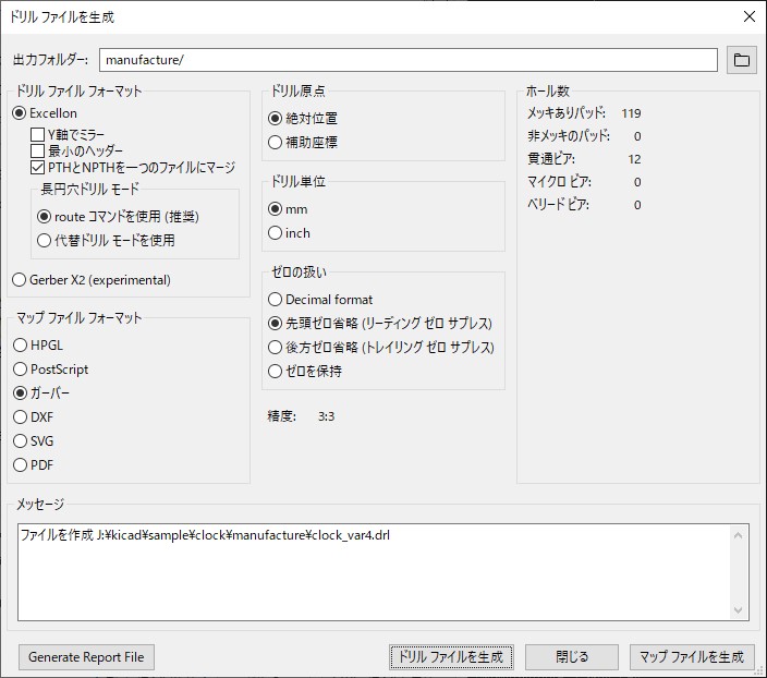
The drill file dialog
Step 2: check the settings
| Setting | Recommended | Description |
|---|---|---|
| Drill file format | Excellon | The standard format |
| Drill units | Millimeters | Millimetres |
| Zeros format | Decimal format | Decimal notation |
| Drill origin | Absolute | Absolute coordinates |
| Drill map file format | Gerber | Map as a Gerber |
Step 3: generate
- Click Generate Drill File
ESP32_Clock.drlappears
Renaming files for JLCPCB (2026 update)
As of 2026 JLCPCB accepts a fairly flexible set of file formats, but these renames are worth doing anyway:
| From | To | Why |
|---|---|---|
xxx.drl |
xxx.txt |
Compatibility with some older systems |
xxx-Edge_Cuts.gbr |
xxx.gml or xxx.gko |
Makes the outline layer unambiguous |
💡 2026 update: current JLCPCB systems recognise .drl as-is, but renaming to .txt removes any doubt.
Creating the ZIP
Bundle the Gerbers and the drill file into a single ZIP.
Files to include:
ESP32_Clock-F_Cu.gbr
ESP32_Clock-B_Cu.gbr
ESP32_Clock-F_SilkS.gbr
ESP32_Clock-B_SilkS.gbr
ESP32_Clock-F_Mask.gbr
ESP32_Clock-B_Mask.gbr
ESP32_Clock-Edge_Cuts.gml
ESP32_Clock.txt (drill file)
ESP32_Clock-drl_map.gbr (optional)
How to zip it (Windows):
- Select all the files
- Right-click → Send to → Compressed (zipped) folder
- Save it as
ESP32_Clock_Gerber.zip
💡 Careful: zip the files, not the folder containing them — the files must sit at the top level of the archive.
Ordering the Board from JLCPCB
Time to order the real thing. This board was made by JLCPCB.
About JLCPCB
JLCPCB is one of the largest PCB manufacturers in the world:
| Item | Detail |
|---|---|
| Price | 2-layer, 100 × 100 mm, 5 boards from $2 |
| Lead time | 24-hour fabrication + 3–7 days shipping |
| Quality | High, built to IPC standards |
| Options | Solder mask colour, surface finish, thickness and more |
| Shipping | From about $15 to Japan (2026); varies by destination |
💡 What this board cost (2026): 5 boards at 200 × 150 mm plus shipping = roughly $30–40.
Placing an order (2026)
Step 1: create an account
- Go to the JLCPCB website
- Sign Up, top right
- Register with an email address (Google sign-in also works)
Step 2: upload the Gerbers
- Click Order Now on the front page

The JLCPCB upload screen (2026)
- Click Add Gerber File
- Select the
ESP32_Clock_Gerber.zipyou just made - Wait for the upload (a few seconds to a minute)
Step 3: check and adjust the board spec
Once the upload finishes, the board dimensions and so on are detected automatically.
A board preview appears so you can confirm everything was read correctly.
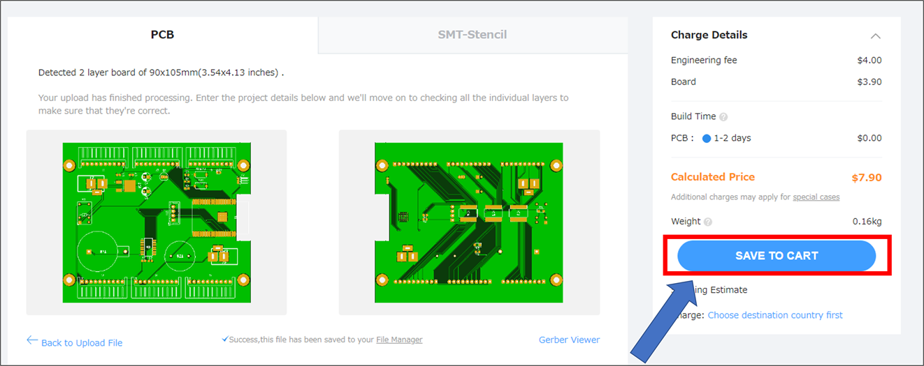
Board preview and specification settings
The settings that matter:
| Item | Default | Recommended | Description |
|---|---|---|---|
| Base Material | FR-4 | FR-4 | The standard substrate |
| Layers | 2 | 2 | 2-layer board |
| PCB Qty | 5 | 5–10 | 5 is the cheapest per board |
| PCB Color | Green | your choice | Green / red / blue / black / white |
| PCB Thickness | 1.6 mm | 1.6 mm | Standard thickness |
| Surface Finish | HASL | ENIG | ENIG is the better finish |
| Copper Weight | 1 oz | 1 oz | Standard copper |
| Remove Order Number | No | Yes | Hides the batch number (+$1.5) |
Worth customising:
- PCB Color: black or blue looks noticeably more professional
- Surface Finish: ENIG (gold) resists oxidation and keeps well
- Remove Order Number: set to Yes and no manufacturing number gets printed on your board
Price: The price updates live on the right-hand side as you change settings. For this board: 2-layer, 200 × 150 mm, 5 pieces = from $7.90.
Step 4: add to cart
- Click Save to Cart
- You are taken to the shopping cart
💡 Handy in 2026: combining several projects into one order saves on shipping.
Step 5: shipping and payment
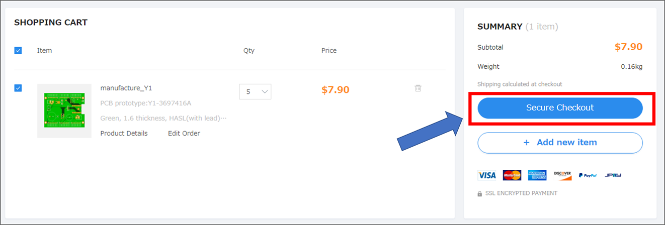
Shipping and payment
Shipping options:
| Method | Cost (2026) | Transit | Tracking |
|---|---|---|---|
| Global Standard Direct Line | free–$5 | 10–20 days | ○ |
| DHL Express | from $20 | 3–5 days | ◎ |
| Registered Air Mail | from $10 | 7–15 days | ○ |
💡 Recommendation: Global Standard if you are not in a hurry, DHL if you are.
Payment:
- PayPal (recommended)
- Credit card (Visa / MasterCard / JCB)
Step 6: address and submit
- Enter your delivery address under Shipping Address
- Check everything one last time
- Click Submit Order
Ordered! 🎉
What happens next (2026)
- Review: JLCPCB checks your board data (a few hours to a day)
- In Production: fabrication starts (1–2 days)
- Shipped: on its way
- Delivered: 3–20 days depending on the shipping method
Tracking: everything is visible under Order History in your account.
A note on import duty
Whether you pay import duty and tax on a small board order depends entirely on where you live — thresholds, handling fees and how the courier processes customs all vary by country. Check your own local rules before ordering, particularly if you are choosing an express courier, since those often add a separate customs handling fee.
Board Ordered — Wrapping Up Part 1
That is the design and ordering side complete.
What this article covered
✅ Circuit design for an ESP32 clock: I/O expanders and an RTC doing the work ✅ Using KiCad 8.x: schematic → PCB layout → Gerber export ✅ PCB design practice: placement, routing, DRC ✅ Ordering from JLCPCB: uploading Gerbers through to payment ✅ Current as of 2026: KiCad 8.x and JLCPCB’s present-day options
What to do while the boards are in transit
Time well spent while you wait:
- Order the parts: get everything on the BOM ordered
- Practise soldering: if it has been a while, warm up on a practice board
- Finalise the firmware: shake the remaining bugs out of the code
- Design an enclosure: 3D printed or wooden, whichever you prefer
Coming next: Part 2
Part 2 is the assembly article. The boards arrive, the parts go on, and the project runs from first power-up through to a finished enclosure.
Related Articles
- I2C vs SPI vs UART: Wiring, Speed, and How to Choose — the I2C bus this board uses, compared against SPI and UART. Explains why the pull-up resistors on this PCB are there, and where the practical limits on trace length come from.
- MCP23017 with ESP32: I2C Address Setup and 16 GPIO Pins — the I/O expander used here, in detail.
- KiCad 10.0 New Features: Importers, Variants, Graphical DRC — what has changed in KiCad since the 8.x release used for this board.
Reference links
See You Next Time! 🚀 Once the boards land, I will see you in the assembly article.